You need to test, we're here to help.

You need to test, we're here to help.
Showing posts with label DDR. Show all posts

17 January 2022

9 Quick Fixes to Improve DDR Probing

Figure 1: Reversed Handsfree mounts and chip clips help relieve strain on fragile solders.
Figure 1: Reversed Handsfree mounts and chip
clips help relieve strain on fragile solders.
Probing at DRAM pins as required by JEDEC can be challenging. Here are nine, simple ways to improve your DDR probing.

1. Use positioning tools to relieve strain on probe tips

The Handsfree probe holder included as an accessory with several Teledyne LeCroy probes, such as the WaveLink and DH Series probes, was originally designed to put weight on the probe tip to ensure a good contact. However, many DDR probing applications utilize solder-in (SI) tips, where the greater concern is to relieve strain on the tip so as to not disrupt the solder. It turns out that if you use the Handsfree in a “reverse mounted” orientation (Figure 1), it puts the amplifier in a perfect position to help relieve strain on probe tips.

04 January 2021

Decision Feedback Equalization in DDR

Figure 1. A transmitted rectangular pulse suffers distortion by the time it reaches the receiver.  Broadening and reflections from previous transmitted bits add to the pulse response,  creating inter-symbol interference.
Figure 1. A transmitted rectangular pulse suffers
distortion by the time it reaches the receiver. 
Broadening and reflections from previous
transmitted bits add to the pulse response, 
creating inter-symbol interference.

High-speed serial links such as those used in DDR4 and DDR5 are subject to a variety of signal degradation challenges.  Insertion losses, frequency dependent attenuation and inter-symbol interference (ISI), as well as others, are among the most commonly encountered sources of signal degradation. 

Figure 1 shows how reflections can cause ISI on a rectangular pulse. When a rectangular pulse is transmitted, it suffers distortion which is apparent when it reaches the receiver.  It may be broadened due to group delay dispersion because different frequency components of the signal propagate along the signal path at differing velocities. In addition, there may be echo pulses, due to impedance mismatches in the channel.  These mismatches cause reflections that propagate back and forth over the channel and appear as these echoes where subsequent bits should be.

14 December 2020

Removing Reflections from DDR Signals Probed Mid-Bus

Figure 1. Virtual probing methods like VP@Rcvr can help remove reflections from signals probed mid-bus.
Figure 1. Virtual probing methods like VP@Rcvr can help
remove reflections from signals probed mid-bus.
Probing DDR signals can present some interesting challenges. The JEDEC specification indicates that all measurements should be made at the output pins of the memory chip. The challenge comes because sometimes the pins of the memory chip are not accessible. You may be able to use an interposer, but even that requires some spatial displacement from the probing point to the Ball Grid Array (BGA) pins of the memory chip. 

If the board has already been populated, there is an even greater problem because the interposer can’t be used, so probes may have to be placed in the middle of the bus in order to make a measurement. In this situation, the probe picks up signals reflected from the memory controller and the memory chip, as well as the desired signals. Reflections appear as non-monotonic ripples on the edges of DQ and DQS signals, as shown in Figure 2.

07 December 2020

Isolating DDR Read and Write Operations

Figure 1. DDR DQ and DQS signals are in phase during a Read operation and out of phase during a Write operation.
Figure 1. DDR DQ and DQS signals are
in phase during a Read operation and
out of phase during a Write operation.
Whether you are debugging or running compliance tests on Double Data Rate (DDR) or Low Power Double Data Rate (LPDDR) memory, the analysis process requires the separation of Read and Write operations to enable measurements on each distinct operational mode. 

The phase relationship between the Data (DQ) signal and the Data Strobe (DQS) signal indicates the type of operation, as shown in Figure 1.

The DQ and DQS signals are phase aligned with edges overlapping in Read mode. In Write mode, they are out of phase, and the DQS edge overlaps the center of the DQ eye.  In the lower speed versions of DDR memory devices, the measuring instrument could be triggered on this phase difference, enabling the isolation of the desired operation for testing.

19 October 2020

Which Virtual Probing Method to Use?


Virtual probing lets you "probe" where a probe can't reach, or compensate signals by deembedding or simulating devices and channels.
Virtual probing lets you "probe" where a probe
can't reach, or compensate signals by deembedding
or simulating devices and channels.
A great feature of Teledyne LeCroy oscilloscopes is the ability to apply virtual probing to compensate an input signal, whether by deembedding fixtures from the signal path, or simulating a “missing” component. It is especially helpful in cases where the signal is difficult to probe at the ideal location, hence the concept of “virtual” probing.

For example, because the JEDEC electrical specifications are defined at the balls of the DDR DRAM, it is often necessary to use the virtual probing capabilities of the oscilloscope to get the best representations of DDR signals to be analyzed with DDR Debug Toolkit or QualiPHY compliance software.

Here, we’ll give an overview of the virtual probing methods that become available with the installation of the SDAIII-CompleteLinQ or VirtualProbe software options, and some guidance as to which method is best to use in which case. And although we’ll show examples drawn from DDR analysis, the benefits of virtual probing are by no means limited to DDR signals.

18 May 2018

Examples of IoT DDR Debug Scenarios

Using the oscilloscope's Track math function can help pin down timing anomalies
Figure 1: Using the oscilloscope's Track
math function can help pin down
timing anomalies
Our last post considered some broad aspects of debugging DDR memory on Internet of Things (IoT) devices, such as how chip interposers can help with probing access and the benefits of virtual probing software. Let's now take a look at some particular examples of problems with these memory chips and their controllers and see how debugging with an oscilloscope might be approached.

15 May 2018

Debugging DDR Memory on IoT Devices

Embedded systems such as IoT devices often require chip interposers to gain access to signal lines on DDR memory
Figure 1: Embedded systems such as IoT devices often require
chip interposers to gain access to signal lines on DDR memory
Internet of Things (IoT) devices are, at heart, just another embedded computing system, albeit one with an extremely well-defined function. As such, there's bound to be some amount of on-board data storage, and the storage medium of choice these days is typically double data-rate (DDR) memory. DDR memory transfers serial data on both the rising and falling edges of the clock signal, which is the characteristic from which it derives its name.

09 February 2018

Probing Techniques and Tradeoffs (Part IX): Best Practices

The typical manner of using a hands-free probe holder can cause issues
Figure 1: The typical manner
of using a hands-free probe
holder can cause issues
Having covered many of the theoretical aspects of probing signals, it's now useful to cover some best practices for high-speed active probing. We'll use some examples involving probing of DDR memory to illustrate what works best and what might not be a good idea from a practical standpoint.

26 July 2017

The Periodic Table of Oscilloscope Tools: Analyze (Part III)

Periodic Table
We're nearing the end of our tour of the Periodic Table of Oscilloscope Tools, our way of presenting our broad palette of oscilloscope tools in a concise, clear fashion. In this installment, we'll finish up the Analyze grouping, by far the largest on the Periodic Table.

19 May 2017

Testing the DDR Memory Interface's Physical Layer (Part IV)

Probes are a key element of the total signal acquisition system
Figure 1: Probes are a key element of the total signal
acquisition system
In this multipart survey of testing the DDR interface's physical layer, we've looked at the basics of the interface itself, a high-level overview of the testing, how to access DDR signals, and read/write burst separation. In this installment, we'll cover preparation for the actual testing.

24 April 2017

Testing the DDR Memory Interface's Physical Layer (Part III)

For analysis purposes. it's critical to separate read and write bursts of interest
Figure 1: For analysis purposes. it's critical to separate
read and write bursts of interest
Last time around, we began examining some of the challenges that come with testing the DDR interface's physical layer. In that post, we concentrated on getting to the devices' physical connections by various means including interposers, backside vias, and DIMM series resistors. Now, presuming we've managed to gain access to the DDR's ball-grid array, the next hurdle is separation of read and write bursts.

11 April 2017

Testing the DDR Memory Interface's Physical Layer (Part II)

A typical BGA package for DDR memory
Figure 1: Shown is a typical BGA
package for DDR memory
In the first of this series of posts, we undertook a high-level view of physical test of a DDR memory interface. Moving forward, let's look into some of the specific challenges one faces in a close examination of these interfaces.

05 April 2017

Testing the DDR Memory Interface's Physical Layer (Part I)

Clock, strobe, and data are three critical signals in DDR test
Figure 1: Clock, strobe, and data are
three critical signals in DDR test
In an earlier post, we took a brief tour through what constitutes a DDR memory interface: clock, command, address, and strobe+data lines linking a memory controller and an array of DRAM memory ICs. Next, we'll examine what DDR interface testing is all about, concentrating primarily on the physical layer.

29 March 2017

Fundamentals of the DDR Memory Interface

A representative test setup for physical-layer DDR testing
Figure 1: A representative test setup
for physical-layer DDR testing
Double data-rate (DDR) memory has ruled the roost as the main system memory in PCs for a long time. Of late, it's seeing more usage in embedded systems as well. Let's look at the fundamentals of a DDR interface and then move into physical-layer testing (Figure 1).

15 October 2014

DDR Memory Testing Part IV: Preparing for Testing

For compliance testing, DDR transition density should be as high as possible
Figure 1: For compliance testing,
DDR transition density should
be as high as possible
The first three installments of this series of posts on DDR memory testing are largely concerned with mechanical issues related to probing, use of interposers, and/or damping resistors. Now, we will turn our attention to the preliminaries of DDR testing itself: generating DDR traffic with which to exercise the memory interface, and criteria for a proper read/write burst pattern that will gain good test results.

08 October 2014

DDR Memory Testing Part III: What Not to Do

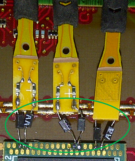
Damping resistors on solder-in probe tips  terminating at chip interposer
Figure 1: Damping resistors on
solder-in probe tips
Testing of dual data-rate memory (DDR) devices and/or modules calls for careful application of some best practices for probing. There will also be cases where the use of chip interposers is called for. Heeding the advice provided in earlier Test Happens posts on this topic will go a long way toward successful probing and testing.

01 October 2014

DDR Memory Testing Part II: Using Interposers

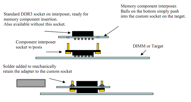
The anatomy of a chip interposer
Figure 1: The anatomy of a chip interposer
If you're a PCB layout designer, you've probably heard one or more test engineers complain: "Why can't you lay out the board so that it can be tested?" All too often, components that need to be accessible to oscilloscope probes are physically inaccessible, whether it's because of close proximity of adjacent components or ball grid array (BGA) mounting of the DUT. It's nearly always a necessary evil, though, because of PCB cost and/or mechanical constraints.

24 September 2014

Eliminate Pitfalls of DDR Memory Testing


DDR test configuration for a desktop computer
Figure 1: DDR test configuration
for a desktop computer
Since its inception as a standard in the mid 1990s, dual data-rate (DDR) SDRAM memory has been near ubiquitous in computing applications. Compared to single data-rate SDRAM, the DDR SDRAM interface makes higher transfer rates possible by more strict control of the timing of the electrical data and clock signals.