You need to test, we're here to help.

You need to test, we're here to help.
Showing posts with label dual-data rate. Show all posts

24 April 2017

Testing the DDR Memory Interface's Physical Layer (Part III)

For analysis purposes. it's critical to separate read and write bursts of interest
Figure 1: For analysis purposes. it's critical to separate
read and write bursts of interest
Last time around, we began examining some of the challenges that come with testing the DDR interface's physical layer. In that post, we concentrated on getting to the devices' physical connections by various means including interposers, backside vias, and DIMM series resistors. Now, presuming we've managed to gain access to the DDR's ball-grid array, the next hurdle is separation of read and write bursts.

01 October 2014

DDR Memory Testing Part II: Using Interposers
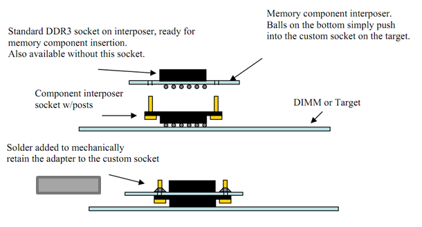
The anatomy of a chip interposer
Figure 1: The anatomy of a chip interposer
If you're a PCB layout designer, you've probably heard one or more test engineers complain: "Why can't you lay out the board so that it can be tested?" All too often, components that need to be accessible to oscilloscope probes are physically inaccessible, whether it's because of close proximity of adjacent components or ball grid array (BGA) mounting of the DUT. It's nearly always a necessary evil, though, because of PCB cost and/or mechanical constraints.