 |
| Figure 1: A representative test setup for physical-layer DDR testing |
A DDR interface entails each DRAM chip transferring data to/from the memory controller by means of several digital data lines. These data streams are accompanied by a strobe signal. Because data can flow both from the controller to the DRAM (write operation) and from the DRAM to the controller (read operation, these digital lines are bi-directional in nature.
 |
| Figure 2: Common clock, command, and address lines link DRAM chips and controller |
DDR is "double data rate" memory because of how data transfers are timed: a byte is transmitted on the rising edge of the clock, and another on the falling edge of the clock. The clock runs at half of the DDR data rate and is distributed to all memory chips.
The DDR command bus consists of several signals that control the operation of the DDR interface. Command signals are clocked only on the rising edge of the clock. Possible command states vary by DDR speed grade but can include: deselect, no operation, read, write, bank activate, precharge, refresh, and mode register set.
 |
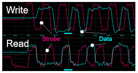
| Figure 3: The timing relationship between the DDR strobe and data signals is different for reads and writes |
Due to the interface's bi-directional nature, data is transferred between the memory and controller in bursts. To that end, the strobe (DQS) signal is a differential "bursted clock" that only functions during read and write operations. In most DDR generations since its inception, the timing relationship between the strobe and data signals is different for reads and writes (Figure 3).
Finally, each DRAM chip has multiple parallel data lines (DQ0, DQ1, and so on) that carry data from the controller to the DRAM for write operations and vice versa for read operations. The data signals are true double data-rate signals that transition at the same rate as the clock/strobe (two transfers per clock cycle).
In the next post, we'll begin an exploration of what goes into physical-layer test of a DDR interface.
No comments:
Post a Comment