 |
| Figure 1: Clock, strobe, and data are three critical signals in DDR test |
Physical-layer tests ascertain whether the voltage levels, timing, and signal fidelities are adequate for a system to function correctly. This is distinct from protocol-layer testing, which determines whether the controller and memory chips are communicating properly at the digital level and above.
Within the domain of physical-layer test are three subcategories:
- Compliance: Do the device output signals comply with the JEDEC specfication?
- Validation: Do the devices interact correctly within the system environment?
- Debug: Why is my device/system not behaving as it should?
 |
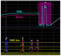
| Figure 2: Analyzing the interplay between the high-speed signals and the command bus deepens insight into DDR behavior |
Which DDR signals are important for such testing? In physical-layer compliance and validation testing, the fastest signals shown in Figure 1 are the most critical: clock (CK), strobe (DQS), and data (DQn). These signals must be analyzed as analog waveforms to fully characterize their signal fidelity. And because there are many data lines in a DDR interface, testing all of them is a time-consuming proposition. Thus, in many instances, board-level simulation reveals the most likely worst-case data lines to isolate them for testing.
 |
| Figure 3: Shown is an example of a complete DDR analysis system |
What would a complete DDR analysis system look like? Figure 3 provides an example. For acquisition of analog signals, a high-bandwidth oscilloscope is paired with low-loading differential probes. Digital signals call for a high-sample-rate digital analyzer and high-bandwidth digital probe. On the oscilloscope, analysis software handles identification of bursts and performs measurements.
In the next installment, we'll begin looking at some of the challenges inherent to DDR physical-layer test.
No comments:
Post a Comment