 |
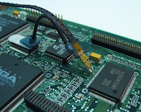
| Figure 1: Reversed Handsfree mounts and chip clips help relieve strain on fragile solders. |
1. Use positioning tools to relieve strain on probe tips
The Handsfree probe holder included as an accessory with several Teledyne LeCroy probes, such as the WaveLink and DH Series probes, was originally designed to put weight on the probe tip to ensure a good contact. However, many DDR probing applications utilize solder-in (SI) tips, where the greater concern is to relieve strain on the tip so as to not disrupt the solder. It turns out that if you use the Handsfree in a “reverse mounted” orientation (Figure 1), it puts the amplifier in a perfect position to help relieve strain on probe tips.
 |
| Figure 2: A gooseneck mounted on another chip supports the tip in good alignment to the pins. |
Finally, a "chip clip" (bottom right Figure 1) can be used to mount the amplifier to the corner of a printed circuit board or the edge of the chassis so that the tip is stabilized. (Note: "Chip clip" is a colloquial term. This is a probe accessory that connects to the amplifier, not the kitchen accessory used to close chip bags).
2. Secure connections
Because of the complexity of DDR probing, it is commonplace to connect probe tips to the board in one location before connecting them to the amplifier in another. Fragile solders can be easily disrupted if the board is shaken or bumped in transit.
To secure probe tips, use Kapton tape, which is especially good because it is insulating and easy to remove. Kapton tape can also be used to secure things that might interfere with the probe, like cables. Don't put Kapton tape on top of damping resistor leads and flex circuit tips, though, because removing it could damage those delicate structures. Best practice is to put Kapton tape below the tip heads, but covering the interconnect leads (Figure 3).
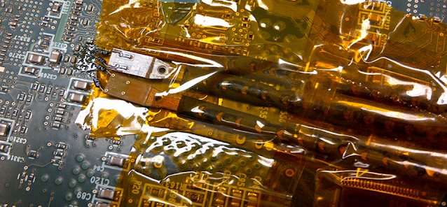 |
| Figure 3: This much Kapton tape may seem excessive, but it is recommended to secure connections if you're moving the board between locations. Just avoid damping resistor leads and flex circuit tips. |
Although it may seem like a good idea because they are designed to protect electronics, do not use an ESD bag to secure boards under test. As the outer surface of some ESD bags acts as a conductor, it could actually make contact with a live portion of the circuit and short it, or else send a signal from one node to another and disrupt the circuit.
3. Use, but don't overuse, hot glue
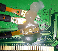 |
| Figure 4: Correct (top two) and incorrect (bottom) placement of hot glue on probe tips. |
It is not recommended to put glue underneath probe tips, as in the bottom of Figure 4, and be careful not to use so much glue you submerge resistors and resistor leads, which can damage the probe.
4. Remove the DIMM from the chassis before connecting tips
It is much easier to solder and secure probe tips if you first remove the DIMM from the chassis. When your board is finished, re-connect the DIMM to the chassis, then connect the tips to amplifiers.
5. Probe the back side of the Ball Grid Array (BGA)
From a signal integrity point of view, the ideal place to probe DDR signals is at the back side of the BGA. This is how JEDEC envisioned DDR testing would be done. However, not every DIMM is a single-ranked DIMM with the BGA ball out accessible from the other side of the board.
6. Use an interposer when the BGA is not accessible
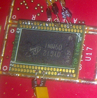 |
| Figure 5: Accessing DDR signals through the pads on an interposer. |
Because it is a fixture that adds its own impedance to the circuit, it is best to use an interposer only when there are no other probing options. Still, the signal integrity is reasonable, and it can be improved if you de-embed the interposer from the signal path. This can be simply done by entering an S-parameter model supplied by the manufacturer into the Eye Doctor II or SDAIII-CompleteLinQ software on the oscilloscope.
Interposers can be difficult to fit onto crowded boards. Some companies even choose to outsource the installation of interposers to others that specialize in just that. When placing an interposer, target a central chip location, so it does not interfere with the clips that secure the DIMM to the main board.
7. Only remove damping resistors if gain accuracy is a problem
Interposers have their own termination, and sometimes interposer manufacturers will recommend that you remove the damping resistors from probe tip leads to improve response. However, removing damping resistors only improves AC response by about 3% and DC response by about 4%, so it only makes sense to do it when the DUT is within 3-4% of passing. If your DUT already has a healthy passing margin, there is no benefit to removing damping resistors—especially if you're sharing probes with others who must replace them on a probe that is now out of spec.
If you believe you must remove the damping resistors, it's recommended to replace them with a 34 gauge wire that's three millimeters in length beyond the PCB edge of the probe tip.
8. Avoid long leads and square pin adapters for high-speed applications
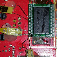 |
| Figure 6: Long, unmatched leads like these only add inductance to the circuit. Avoid lengthening leads to reach difficult probing points, use positioners instead. |
Square pin adapters minimize inductance, but they usually have only about a 3 GHz bandwidth rating, limiting them to low-speed DDR2 signals, whereas SI probe tips are often rated much higher. Avoid using square pin adapters for any applications over 3 GHz.
9. Always ground the probe when measuring floating signals
All active differential probes, such as you would use for DDR probing, have a peak differential mode range and a common mode range that is referenced to ground. If the signal measured is a floating signal that is not earth grounded, it can float out of and exceed the probe's common mode range.
 |
| Figure 7: Characteristic "pinched" trace that occurs when the signal floats outside the probe's common mode range. |
You can earth ground the floating device simply by hooking an alligator clip, or the ground lead supplied with the probe, to where the DUT would normally be grounded.
Mike Hertz teaches more ways to improve DDR probing in our on-demand webinar, Top Tips and Techniques for DDR Probing and Testing.
See also:
Probing Techniques and Tradeoffs (Part IX): Best Practices
Probing Techniques and Tradeoffs (Part X): More Best Practices
Testing the DDR Memory Interface's Physical Layer, Part II
Eliminate Pitfalls of DDR Memory Testing
No comments:
Post a Comment