 |
| Figure 1: Embedded systems such as IoT devices often require chip interposers to gain access to signal lines on DDR memory |
 |
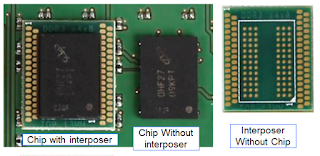
| Figure 2: Interposers reside between the ball-grid array on the bottom of a DDR chip and the PCB's solder pads to make signal lines more easily accessible to probing |
Interposers come into play with DDR memory chips on IoT devices because such chips are often made in ball-grid-array (BGA) packages, which renders the signal pins inaccessible. Figure 2 shows DDR chips with and without an interposer as well as an interposer without chip attached. From these images, you get the idea of what the interposer does, which is to bring out formerly inaccessible signals so that they can be probed with relative ease.
 |
| Figure 3: A side view of a chip interposer provides a better look at its mechanical function |
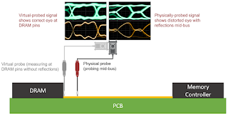
The JEDEC standard for DRAM testing requires that the device be probed directly at its pins. Alas, at times not even interposers can make this possible. You end up having to probe the signal line somewhere mid-bus rather than at the terminated DRAM chip. Say, for instance, that a read signal emanating from the memory chip is probed mid-bus. The probe picks up some of that signal, but it also continues down the trace to the memory controller, where it reflects back to the probe as a phase-shifted, amplitude-attenuated version of itself and gets mixed in with what the probe is picking up.
 |
| Figure 4: Virtual-probing software running on the oscilloscope can remove reflections from mid-bus probing of the bus |
There are two ways in which the virtual-probing software can approach the elimination of mid-bus probing reflections. One is to use S-parameters to model the signal path and remove the reflections through S-parameter modeling. If S-parameters are unavailable, another approach is to use simulation to arrive at RLC models of parameters such as skin effect and delay.
A final post to come will look at some concrete debug steps for IoT DDR memory.
Previous blogs in this series:
Debugging the IoT
Anatomy of an IoT Device
IoT Digital Power Management and Power Integrity
Investigating IoT Wireless Signals
Investigating IoT Wireless Signals (Part II)
Acquiring and Characterizing IoT Sensor Signals
Debugging Low-Speed Serial Data on IoT Devices
Debugging CANbus for IoT Devices
Debugging Ethernet, SATA, and PCIe for IoT Devices
No comments:
Post a Comment