 |
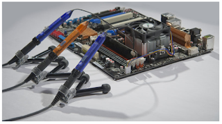
Figure 1: Probes are a key element of the total signal
acquisition system |
In this multipart survey of testing the DDR interface's physical layer, we've looked at the
basics of the interface itself, a
high-level overview of the testing, how to
access DDR signals, and
read/write burst separation. In this installment, we'll cover preparation for the actual testing.
The first matter to consider is the oscilloscope to be used for the testing. Testing DDR interfaces always means using probes, so it's a good idea to look at the oscilloscope and probes as a complete acquisition system (Figure 1). Critical attributes of that system include a) adequate bandwidth, b) low loading, and c) easy mechanical connection to the DUT. Let's look at each of these attributes in turn.
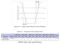
Conventional wisdom dictates that "oscilloscope bandwidth should be at least five times the bit rate. However, DDR interfaces have very fast slew rates relative to their transition rates (Figure 2). Thus, characterizing the system with acceptable rise-time accuracy demands an oscilloscope and probe pairing with a relatively high bandwidth.
 |
Figure 2: The high slew rates of DDR
interfaces boost bandwidth needs |
Probe loading takes the blame for a great many observed issues when using oscilloscopes, and not just for testing DDR interfaces. In a large majority of instances, signal fidelity problems can be traced to the signal path within the probe itself. Probes with insufficiently low loading are much more likely to cause functional failures in devices. Teledyne LeCroy's
WaveLink Dxx30 differential probes present one good option for DDR applications.
In the vast majority of DDR test applications, solder-in probe tips make the mechanical connection to the DUT. Because of the many signals being probed, these tips must be of sufficiently small size. They should also offer physical flexibility to reduce torque on the relatively delicate solder connections as the probe amplifier is moved. Finally, they should serve several different types of measurement tasks to reduce the complexity of test setup.
 |
Figure 3: Poor usage of the oscilloscope's dynamic range
reduces the SNR, while clipping the signal can result
in an overdriven front end
|
So with an oscilloscope and probes ready to go, the next step in preparing for testing the DDR interface is to deskew the probes. Deskewing is a critical step in all applications involving probes and timing measurements, but even more so for DDR measurements. The importance of the DQ/DQS phase in many of these measurements imparts a particular sensitivity to skew issues. When the probing points are in close proximity to each other, all probes can be deskewed to the same reference plane.
Deskewing becomes more critical when practicality dictates that one signal must be probed at some physical distance from others. In such instances, propagation delay becomes a factor. There are three principal means of determining propagation delay: simulation, rules of thumb (such as 140 ps of delay/inch), and aligning signals known to be synchronous. This latter approach risks masking of any genuine skew problems in the DUT.
 |
Figure 4: Best practices include separating signals into
their own respective grids and setting vertical gain so
that signals occupy about six vertical divisions |
Another important item in preparing for DDR measurements is to maximize the oscilloscope's dynamic range (see
"Don't Leave Oscilloscope Performance on the Table" for more tips). In Figure 3, the signals occupy only about 50% of the display grid, which reduces signal-to-noise ratio by about 6 dB. Moreover, the top-most signal is "clipping" and could be overdriving the oscilloscope's front-end amplifier.
Figure 4, on the other hand, illustrates some best practices (not only for DDR measurements but for all oscilloscope applications). Rather than leaving the display as a single large grid, it is better to separate the signals into their own respective grids. Avoid signal clipping by setting vertical gain so that the signals occupy about six vertical divisions. These two practices will give you the maximum usage of your oscilloscope's dynamic range.
 |
| Table: Specified signal levels for DDR variants |
Finally, make sure the signal levels appear as specified for the DDR variant you are working with (see the table). Many automated measurements depend on the basic settings being correct. If the signal levels seem incorrect, it could be due to a probing problem, such as using the wrong reference, or a device/system problem, such as an incorrect V
dd or V
ref.
Heeding the above advice should make for smoother sailing in the waters of testing a DDR interface's physical layer.


No comments:
Post a Comment