 |
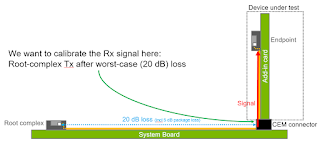
| Figure 1: PCIe 4.0 receiver link-equalization testing takes place at the site of the channel's worst-case signal |
The calibration process for this test can be a bit daunting. We do so by emulating the entire 28-db worst-case channel and calibrating for a worst-case signal at the receiver chip of a 4.0-compliant add-in card. Then we remove that card's 8-dB loss from the system and plug in the actual DUT. So this means we've calibrated for a worst-case add-in card channel. If you end up having only 6-dB loss in the DUT, congratulations! You've bought yourself 2 dB of loss margin.
As with most modern receiver test procedures, the idea here is to create a minimum-compliance eye, or a worst-case-compliant eye, at the receiver. We do so by creating a worst-case-compliant eye at the output of the transmitter and then feeding that signal through a worst-case channel.
To create the worst-case-compliant eye at the transmitter, we put our BERT into service. We don't put a channel in place just yet, but rather connect the output of the BERT directly to the oscilloscope. The BERT will be acting as the Tx chip in a real channel. We first need to calibrate each Tx emphasis preset in our "transmitter," checking them with the oscilloscope to be sure that the preshoot and de-emphasis values match what they should be in a PCIe 4.0 transmitter.
A compliant PCIe 4.0 transmitter is permitted a maximum 1 ps RMS of Rj and 0.1 unit intervals (UI) of deterministic jitter. We set those values using the BERT's jitter generators and then check them on the oscilloscope using PCI-SIG's SigTest software to ensure that we are generating a worst-case-compliant eye at the transmitter output.
 |
| Figure 2: Shown is the PCIe 4.0 receiver test calibration setup |
Referring to Figure 2, we'll pipe a 2-GHz sinusoidal noise signal through a compliant 28-dB channel. The oscilloscope, acting as our "receiver," should see that signal as a 14-mV sinusoidal noise signal. However, at 2 GHz, that whole channel has about 6 dB of loss. So we can't simply set 14 mV at the BERT and expect to see that at the oscilloscope at the far end.
We're looking for an transmitted eye with a very specific amount of vertical and horizontal opening with which to conduct our receiver test. We want to get as close as possible to that amount of eye opening using channel loss before we begin adding noise and jitter to finally close the eye to the exact values.
 |
| Figure 3: Connection schematic for eye calibration |
One way in which we achieve that maximally closed eye is by varying the loss in the channel between 19 and 22 dB, which results in anywhere from 27 to 30 dB of total channel loss.
We'll continue with this topic of PCIe 4.0 receiver link-equalization testing in our next post.
Earlier posts in this series:
Introduction to PCIe 4.0 Electrical Compliance Test
Gearing Up for PCIe 4.0 Electrical Compliance Test
PCIe 4.0 Transmitter Electrical Testing (Part I)
PCIe 4.0 Transmitter Electrical Testing (Part II)
PCIe 4.0 Transmitter Link-Equalization Testing
No comments:
Post a Comment