 |
| Figure 1: PLL bandwidth testing ensures that the add-in card's PLL bandwidth and peaking are within specifications |
 |
| Figure 2: Shown is the connection schematic for the PCIe 4.0 PLL bandwidth test |
 |
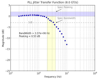
| Figure 3: Plotting a curve of the jitter transfer for each frequency |
The results are obtained by simply plotting a curve of the jitter transfer for each frequency, and comparing the results to the specification limits (Figure 3).
This completes our overview of the PCIe 4.0 compliance tests, at least until there is more information to share regarding the tests still under definition, which include: transmitter pulse-width jitter, lane margining timing, and lane margining voltage (Figure 1, again). We'll provide a post updating this series at that time.
Earlier posts in this series:
Introduction to PCIe 4.0 Electrical Compliance Test
Gearing Up for PCIe 4.0 Electrical Compliance Test
PCIe 4.0 Transmitter Electrical Testing (Part I)
PCIe 4.0 Transmitter Electrical Testing (Part II)
PCIe 4.0 Transmitter Link-Equalization Testing
PCIe 4.0 Receiver Link-Equalization Testing (Part I)
PCIe 4.0 Receiver Link-Equalization Testing (Part II)
No comments:
Post a Comment