 |
| Figure 1: Wide-bandgap (GaN) power semiconductor device waveforms captured using two, different probe topologies. Click on any image to expand. |
Why are power semiconductor device measurements challenging?
- It is relatively easy to measure the lower side power semiconductor devices (MOSFET or IGBT) because they are referenced to ground. Single-ended passive probes can be used but are not recommended because it is easy to carelessly probe a high-voltage portion of the circuit and damage the probe, oscilloscope or the device under test, or cause harm to the operator.
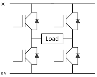
- It is harder to measure the upper side power semiconductor devices because they are referenced to a voltage that is non-zero. This is called a floating measurement. This precludes use of the ground-referenced single-ended probes, as they would short circuit the DUT. This measurement requires a high-voltage differential or single-ended isolated probe.
- The upper side power semiconductor device measurements benefit from the high common-mode rejection ratio (CMMR) of an optically isolated probe, like the DL-ISO or Tektronix® IsoVu™, to help resist switching interference from the lower side devices.
- When measuring wide-bandgap devices, such as Gallium-nitride (GaN) and Silicon-carbide (SiC), high bandwidth may also be desired to accommodate the faster rise times supported by these devices.
Measuring both upper and lower power semiconductor devices simultaneously gives complete insight into the design’s behavior. In addition to evaluating the switching losses, designers will evaluate the timing to learn if there is sufficient dead-time margin to preclude any possibility of both upper and lower devices being turned on at the same time, which would cause a short circuit (shoot through). So, it's essential to have a probe that can perform adequately for the upper side measurements.
Choosing with the High-voltage Probe Selection Guide
 |
| Figure 2: Topology of a full-bridge wide-bandgap (GaN) transistor. |
Based on this information, we make three, simple selections on the High-voltage Probe Selection Guide (Figure 3):
- DC Bus Voltage = 170 – 1000 Vdc
- Semiconductor Device Material = Wide-bandgap (SiC or GaN)
- Applications = Power Semiconductor Testing
 |
| Figure 3: Selections for testing on a 260 Vdc bus wide bandgap (GaN) transistor. |
The Guide chooses the DL-ISO Series High-Voltage Optically Isolated Probe as the best probing option (green) for the gate drive and switching loss measurements.
The HVD Series High-Voltage Differential Probe is a better option than a single-ended passive probe, but it may cause circuit loading due to its input capacitance. It may also have insufficient bandwidth for the faster wide bandgap devices, especially the GaN device used in the example. There are compromises in using this type of probe, but some users may find that the probe works fine for their particular measurement needs.
One reason the DL-ISO is the best option is the probe’s CMRR. The DL-ISO series has a CMRR of 160 dB at DC and significantly higher CMRR than the other probes at higher frequencies. The HVD probe has a CMRR of 85 dB at DC and 65 dB at 1 MHz. While the HVD Series probe has excellent CMRR for a conventional HV differential probe, and may perform acceptably well depending on the device and the circuit, CMRR is not as good as DL-ISO, and it has much less than 1 GHz bandwidth.
Finally, the DL-ISO Series offers up to 1 GHz bandwidth to match the requirements of GaN devices. The HVD Series probes have a bandwidth of up to 400 MHz, corresponding more closely to the bandwidth requirements of SiC or Silicon (Si) power semiconductor devices.
The best choice for this type of power device measurement is the single-ended, fiber optically isolated probe. Its single-ended configuration minimizes loading, which offers the benefit of better signal fidelity. The probe isolation circuitry is less susceptible to picking up transients. It has better CMRR at high frequencies, which is important for circuits using wide bandgap semiconductors such as the GaN MOSFETs in this example. This, combined with the probe’s isolation circuitry, results in more accurate upper side measurements.
Real-world Capture Comparison
To prove the point, let’s compare Vds (MOSFET Drain-Source) signals captured using a DL-ISO probe and an HVD probe (Figure 1). The DL-ISO probe (magenta trace) is connected to the gate of one of the upper side MOSFETs. The HVD probe (blue trace) is connected to the gate of the other upper side MOSFET. This allows simultaneous observation without the probes affecting each other by loading the circuit, which would happen if they were connected to the same measurement point.
Note that the HVD probe exhibits a small overshoot on the edge transitions. This overshoot is most probably due to the lower CMRR of the HVD probe compared to the DL-ISO. There is no discernible overshoot visible in the signal from the DL-ISO probe. The optical coupling of the DL-ISO probe provides the best CMRR performance, which helps to suppress electrical transients coming from elsewhere in the circuit.
To try the High-voltage Probe Selection Guide, visit: teledynelecroy.com/powerprobes
See also:
How to Choose the Best High-voltage Probe in 5 Min.
No comments:
Post a Comment