 |
| Figure 1: This cross section of a 100-MHz microstrip transmission line shows us how a return path should look |
Why is ground bounce such an insidious problem? For one thing, it's hard to pin down without using a "trick" like sense lines. It scales with shorter rise times and larger Δi/Δt. It scales with more simultaneous I/O switching. The larger the discontinuity in the return path, the larger that impedance, and the larger the ground-bounce voltage. It's a major problem with asynchronous buses.
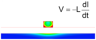
Ground bounce is caused by two fundamental elements. First, the return path is poorly designed. Instead of a wide, continuous plane, we've managed to design a highly restrictive return path. Figure 1 is an example of the cross section of a 100-MHz microstrip transmission line, with the colors showing where current is flowing. Blue means no current; others mean more current flow. The cross section shows the return current for this signal line flowing in the return path underneath the conductor. Most of that current flows directly below the conductor, but it spreads out a bit on either side. You can eliminate all of the return-path conductor to the far right and left (solid blue) and not affect the return path. It's when you encroach into this region where there's return current that you affect the signal and affect the return path.
If your return-path conductor distorts the return current so that it's narrower than the green-tinged region in Figure 1, maybe because the return path is a package lead or a connector trace, or if you design that return path for any reason to narrow it in that way, you will have increased the discontinuity in that return path and increased its inductance. That's the first ingredient in the ground-bounce recipe.
The second ingredient that makes ground bounce happen is if you also have more than one signal sharing that return path. It's the voltage noise created by one signal in that higher-inductance return path that another signal will see if it's sharing it. The combination of a badly-designed return path that has higher inductance than it should and more than one signal sharing it guarantees that we will have ground bounce.
 |
| Equation 1: Shown is the "golden relationship that determines how much ground bounce will happen in a return path |
If we know what causes ground bounce—common lead inductance, shared return paths, and Δi/Δt in those shared return paths—we can calculate how much of it we expect to see and what parameters in our design are influencing it.
The "golden relationship" shown in Equation 1 tells us everything we need to know about ground bounce. It says that the voltage noise we will see on that common lead inductance of the return path comprises the total inductance of that return path as dictated by its geometry, the number of simultaneously switching I/Os that share that path, and the Δi/Δt seen by each of those I/Os. If we want to reduce the ground bounce voltage, these are the design knobs we have to turn to make that happen.
We want to make the total inductance smaller and reduce the number of I/O lines sharing a return path. In addition, we want to make the Δi that switches smaller and to make the "t" in the Δt larger.
- Ltotal: Design short and wide return conductors, keep signals close to return paths, and use planes with thin dielectrics for power/ground paths
- n: Simple: Don't share return paths!
- Δireturn current: Stagger I/O switching, use source series termination resistors, use more return paths, and use differential signals
- Δt: Always use the longest rise time that will keep you within your timing budget, and use slew-rate control.
Even if you use differential signaling, you still want to reduce mode conversion as much as possible. Mode conversion will create common current that will drive some ground bounce. When it comes to Δt, a longer rise time is rarely an option, but always look into it as a possibility.
This concludes our series of posts on ground bounce. Hopefully, it's helpful to you in your quest for ever-improving signal integrity.
This concludes our series of posts on ground bounce. Hopefully, it's helpful to you in your quest for ever-improving signal integrity.
Previous posts in this series:
About Ground Bounce and How to Measure It
More on Quiet-Low I/O Drivers and Ground Bounce
A Walk-Through of Ground-Bounce Measurements
No comments:
Post a Comment