 |
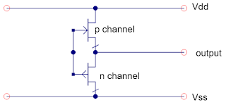
| Figure 1: To configure an I/O driver as a quiet-low line, its output is connected directly to Vss on the die |
As we discussed in our last post on this topic, ground bounce happens when multiple I/O drivers share common Vdd and Vss lines AND return paths are not wide, uniform planes, resulting in higher total inductance in the return path. That inductance, in turn, causes a voltage difference between the ends of the common lead, the polarity of which depends on whether drivers are switching high-to-low or low-to-high at any given time.
Figure 1 shows us a simple schematic of an I/O driver for reference. Typically, I/O drivers are CMOS devices with p-channel and n-channel junctions that drive the I/O line. We want to fix this driver's output in a low logic state, and to do so, we turn on the n-channel gate in the output and turn off the p-channel gate. We connect the output of the driver directly to Vss on the die with a low-impedance connection.
It's important to bear in mind that, from a signal-integrity standpoint, while we tend to think of interconnects in circuits like these as simple "wires," they actually have electrical properties. In particular, the minuscule return path between the die and the host PCB has a good deal of inductance. But once the return currents of those signal lines reach the solder ball to the ground plane in the board, the inductance of the path to the signal-transmission lines has very low inductance. Once the signal enters the board-level transmission line, the signal and its return propagate on a uniform transmission line. This is what makes it possible for us to use our quiet-low I/O driver to tell us what's going on voltage-wise with Vss on the die vs. Vss on the PCB.
 |
| Figure 2: For demonstration purposes, here's how we configured the I/Os on an Arduino MCU |
Let's take a look at how this little quiet-low I/O trick is implemented in practice on a microcontroller (Figure 2). This schematic represents an Arduino MCU that's been instrumented such that there's only one Vcc and Vss connection shared by all of the I/Os. Also, the Vdd, or core-logic power supply, shares the same rail. So, by using a quiet-high for one of the outputs, we can sense not only the Vcc, which is the power supply for the I/O ring, but also the Vdd core-logic supply.
Thus, our quiet-high sense line lets us monitor what's happening with the Vdd rail on the die even as it comes out to a quiet-high transmission line on the PCB, where we have coaxial cables connected to it on the board that bring its signals to an oscilloscope. Meanwhile, a quiet-low I/O driver senses the noise getting through the inductance and resistance of the die's package leads on the die's Vss rail, enabling its comparison to the board-level ground.
For demonstration purposes, one I/O driver serves as a trigger that will switch at the same time as the other drivers. To ensure that the trigger I/O doesn't draw a lot of current, there's a 450-Ω series resistor in that path. From there, the signal is fed directly to a 50-Ω oscilloscope input using a high-bandwidth cable. The two resistances of 500 Ω total draw only about 10 mA from the I/O ring, so that trigger I/O will generate a bare minimum of ground bounce itself. To evaluate the real ground bounce of the switching I/Os, we'll sequentially trigger one I/O at a time, and then both at once.
In an upcoming post, we'll look at the results of our demonstration.
Previous posts in this series:
About Ground Bounce and How to Measure It
No comments:
Post a Comment