The diagram of the USB-C receptacle in Figure 1 shows where it potentially switches from normal operation into Alt-Mode.
You need to test, we're here to help.
13 December 2021
USB4 Alt-Mode Testing: DPAUX and USB-PD
06 December 2021
Testing DisplayPort 2.0 vs. USB4 Over USB Type-C Connectors
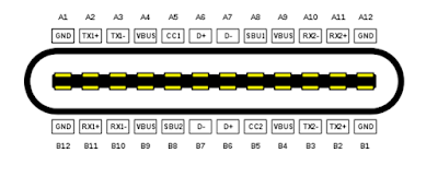 |
| Figure 1: The pin out of the USB Type-C connector. |
DisplayPort™ 2.0 (DP 2.0) is a high-resolution video interface and USB4® is a high-speed data interface; what they have in common is the USB Type-C® (USB-C) connector. While DP 2.0 can also be deployed on the standard DisplayPort as well as mini-DisplayPort connectors, it is the USB-C connector that really excites electronics manufacturers because now they can use a single connector for high-speed data, high-resolution video and even power distribution.
Figure 1 shows the pin assignments for a USB-C connector, which is a mechanically reversible connector that includes four, high-speed differential data lines: TX1, TX2, RX1 and RX2.
In USB4 operations, the four data lines TX1, TX2, RX1 and RX2 form a dual-lane, duplex signal path, supporting 10 and 20 Gb/s transfers on each line. When operating in USB4 Alt mode, up-to-four of these buses can be reassigned to become four DP 2.0 video lanes, which operate at 10, 13.5 or 20 Gb/s.
Testing for both interfaces over the USB-C connector is similar, but there are some notable differences.
29 November 2021
DisplayPort 2.0 Physical Layer Testing
 |
| Figure 1. Functional diagram of DisplayPort 2.0 over USB-C Source (Tx) PHY testing. |
The Video Electronics Standards Association (VESA) DisplayPort 2.0 video interface introduces a new performance standard with an increase in data bandwidth of three times compared to the older DisplayPort 1.4a specification, achieved by using four lanes of up-to-20 Gb/s data per lane. This permits display resolutions to better than 8K, higher refresh rates and better dynamic range. These advantages are available using native DisplayPort connectors as well as the USB Type-C connector, which allows devices to handle video data, USB data and power all in the same connector.
22 November 2021
What Is Differential Manchester Encoding?
 |
| Figure 1. Differential Manchester encoding is based on the presence or absence of a transition, whereas Manchester encoding relies on the polarity of the transition. |
Manchester is categorized as bi-phase encoding because the signal is checked twice every bit interval, also called self-clocking. Each check is one “tick”, each bit interval equals two ticks of the clock. This removes the need for the separate clock signal that is required for Non-Return to Zero (NRZ) encoding. Instead, data and clock signals are combined into a single, two-level, self-synchronizing data stream. The clock can be "extracted" by measuring the timing of the edges.
 |
| Figure 2. In Manchester encoding, the polarity of the transition that occurs mid-interval determines the logic. |
 |
| Figure 3. Even inverted, DME signals result in same logic. |
DME is used for 10Base-T1S Automotive Ethernet, a short-distance, low-bandwidth application with either a point-to-point or bus topology up to 25 m.
Teledyne LeCroy offers QualiPHY compliance test solutions for 10Base-T1S, including a QPHY-10Base-T1-TDR option that automates all required MDI S-parameter tests using the WavePulser 40iX.
For more information about 10Base-T1S compliance testing, see the on-demand webinar, How to Become an Expert in Automotive Ethernet Testing, Part 1.
See also:
Automotive Ethernet in the Vehicle
Fundamentals of Automotive Ethernet
15 November 2021
Using Tracks to Demodulate Frequency/Phase Modulated Signals
 |
| Figure 1: A low-pass filtered track of the Frequency measurement demodulates the linear frequency sweep in a radar chirp. The frequency domain FFT shows the range of the frequency change. |
08 November 2021
Finding “Unknown” Waveform Anomalies
 |
| Figure 1: Width “exclusion” trigger captures pulse widths outside the range of 980 ns to 1 µs. The first anomaly captured is a width of 2.99 µs. |
Look for What’s “Not Normal”
A simple approach is to measure the nominal waveform, then trigger the oscilloscope on waveform elements that differ from nominal. Figure 1 shows a 500 kHz square wave with a roughly 50% duty cycle, so the pulse width is normally about 1 µs (the Width measurement shows a mean of 997 ns). This nominal width does not change significantly with any regularity and gives us a basis on which to begin looking for anomalies.
01 November 2021
Finding Intermittent Events
 |
| Figure 1: Statistics for 1261 Width measurements taken over 97 acquisitions on the Measure table. Width statistics can help determine the set up of a Glitch SmartTrigger. |
25 October 2021
Measuring Dead Time in 48 V Power Converters, Part 2: Dynamic Measurements
 |
| Figure 1. P1 and P2 measure dt@lvl over the entire acquisition, while P3 and P4 measure dt@lvl for only a single operational cycle of zoom traces Z1 and Z3. |
As we learned in part 1, the dead time delay is measured using two instances of the measurement parameter Delta Time at Level (dt@lvl) as shown in Figure 1.
In the Figure 1, the dt@lvl parameters P1 and P2 show the value of the last measurement in the acquisition which contains 10,000 switching transitions. The parameters P2 and P4 measure only the single timing cycle shown in the zoom traces. (Click any image to enlarge it and see the detail.)
The values of both parameters are different, and you should ask the question: how does dt@lvl vary with time? To find the answer, turn on the measurement parameter statistics, as shown in Figure 2.
18 October 2021
Testing for Near Field Radiated Emissions in the Time Domain
 |
| Figure 1. Triggering on a time-domain signal likely to be coincident with radiated emissions helps to locate where in the channel di/dt occurs. |
2. Physical structures that are not tightly coupled to the return plane
3. Ground loops causing common currents in cables
We’ll briefly demonstrate a bench top test for finding sources of near field radiated emissions caused by return path discontinuities using a real-time oscilloscope in the time domain.
Why the time domain? Although EMC compliance testing is done in the frequency domain, in the time domain we can see the signatures of near field emissions in a way that yields information about the root causes of those emissions. It is a type of pre-compliance EMC testing that can be easily done in your lab, without the expense of an anechoic chamber.
11 October 2021
Near Field vs. Far Field Radiated Emissions
 |
| Figure 1. The near-field emissions we measure in the lab may not be an accurate measure of the far-field emissions on which EMC is certified. |
04 October 2021
Unintentional Antennas in Electric Circuits
 |
| Figure 1. Certain design features can introduce unintentional antennas into electric circuits. |
Where do these radiated emissions come from? No one designing an electric circuit board is designing them into their product on purpose. These sneaky antennas do not appear in the schematic. However, we can unwittingly introduce them into our product through certain styles of board and interconnect design features. It is sometimes jokingly said there are two kinds of designers: those who are designing antennas on purpose, and those who aren't doing it on purpose. We’re going to introduce two, basic models of antenna—magnetic dipole and electric dipole (Figure 1)—to reveal a secret source of radiated emissions.
27 September 2021
Pre-compliance EMC Testing Using a Real-time Oscilloscope
 |
| Figure 1. Formula for calculating radiated power from electric field measured at a given distance. Only a few nanowatts of radiated power can cause a product to fail an EMC certification test. |
Problems with signal integrity, power integrity and EMI all come to life when we turn that schematic into a physical implementation, because once we have connectivity established by the interconnects, the only thing interconnects are going to do is screw up our beautiful design. They're going introduce noise, and that noise is going to cause some combination of signal integrity, power integrity and EMI problems. The best we can do is to minimize its appearance and impact using best design practices.
In this series, we'll focus on design issues that affect EMI, and how you can use a real-time oscilloscope to find the root causes of EMI that negatively affect a product's electromagnetic compatibility (EMC).
20 September 2021
Testing Power Rail Sequences in Complex Embedded Systems
 |
| Figure 1. Four power rail signals on a single grid, with cursors measuring the time delay between the first pair in the sequence. |
13 September 2021
Correlating Sensor and Serial Data in Complex Embedded Systems
 |
| Figure 1: Voltage output of a temperature sensor. As the temperature rises, the output voltage falls. |
Where it is possible to probe the temperature sensor, the output is a DC signal that changes very slowly over time. Figure 1 shows a direct measurement of the temperature sensor using a heavily filtered oscilloscope channel to minimize noise pickup.
07 September 2021
Correlating Low to High-Speed Events in Complex Embedded Systems
 |
| Figure 1: A challenge when testing embedded systems is to correlate events in a low-speed interface like SPI to events in a high-speed interface like PCIe. |
Take for example testing the initialization of the system. When power is first turned on, the ROM bios and flash memory initialize program elements that are required by the embedded system’s microprocessor. Once the initialization is complete, the microprocessor has to notify the motherboard via PCIe that it is active and ready to receive data via the high-speed serial bus. This all has to happen within 200 milliseconds.
30 August 2021
Debugging Complex Embedded Systems
 |
| Figure 1: A typical embedded system has many devices utilizing a wide range of signal types and bandwidths. |
Let's start by defining what we mean by embedded system and deeply embedded system. For our purposes, an embedded system is a fixed function, self-contained control system on one printed circuit board. Typically, printed circuit boards (PCBs) will have multiple passive devices, a few active electronic devices, analog devices, digital devices and a few serial data devices. There tends to be a microcontroller device to process data and control other components. There will also be some type of system memory, often embedded inside the microcontroller. And, there will be some power conversion devices and power distribution elements that power all the other devices in your embedded system.
23 August 2021
Measuring Dead Time in 48 V Power Conversion Systems, Part 1: Static Measurements
48 volt power conversion systems input a 48 VDC power bus and output other voltage levels. The key section in the conversion process is the inverter stage. The inverter subsection topology may be half bridge, full or H-bridge, or cascaded H-bridge for 3-phase systems. There is typically a filtering circuit after the inverter before power is passed on to the Load, and a control system that takes care of controlling the entire conversion system.
The three inverter topologies shown in Figure 1 are all similar in that they use stacked or “totem pole” power devices for switching.
In operation, each of these topologies provides a path from the DC bus through the load and then to ground (0 V) by turning on selected devices. At no time should there be a direct path from the DC bus to ground, an event called “shoot through.” Designers intentionally add dead time to eliminate the risk of shoot through.
09 August 2021
Debugging Dynamic Link Behaviors with CrossSync PHY for PCIe
 |
| Figure 1: These upstream lanes show unexpected equalization behavior. If you only had the electrical signals to work with, how would you begin debugging them? |
At PCI Express compliance events, or when doing pre-compliance testing in the lab, a transmitter link equalization test is performed to determine whether a device is capable of correct link equalization in isolation. A piece of test equipment, usually a protocol-aware BERT, acts as the link partner for the device under test. The BERT requests specific preset changes from the device, in response to which the device (in theory) changes its preset to provide the correct channel compensation. The changes are captured by an oscilloscope, which is capable of visualizing the transmitter equalization changes in the electrical layer and measuring first of all, if they happen quickly enough, and secondly, if the device actually changed to the preset levels requested, which occur in a known sequence.
But what happens when you suspect "weird" equalization behavior in a live link between two devices—for example, something off with the upstream equalization in Phase 3? How would you capture that to begin debugging the problem? Where would you look for a clue as to what is happening?02 August 2021
Debugging L1 Substates Timing Errors with CrossSync PHY for PCIe
 |
| Figure 1: CrossSync PHY for PCIe lets you easily map the electrical to the protocol layer of L1 substate events. |
26 July 2021
Anatomy of a PCIe Link
 |
| Figure 1: A PCIe link between root complex and end point. Each device has its own transmitter and receiver. |
19 July 2021
How to Test Noisy Power Supply Outputs
 |
| Figure 1: 3.3 V output of a DC-DC converter. The waveform shows the nominal DC level, ripple and high frequency noise bursts. |
In this post, we'll discuss how the choice of probe affects the noise present in power measurements, as well as how oscilloscope settings such as termination impedance, bandwidth and coupling can be adjusted to lessen noise and improve measurement results.
Figure 1 shows a typical DC-DC converter output measurement. The mean value of the waveform is 3.294 V. Ripple appears at the switching frequency of 1.2 MHz, and noise in the form of high frequency bursts and baseline thickening is visible throughout.
Waveforms like this can be acquired with a 10:1 high impedance probe, a 1:1 coaxial cable connection, or a 1.2:1 rail probe using either DC or AC coupling, as available. Figure 2 summarizes how each oscilloscope/probe configuration affects the measurement.
12 July 2021
MAUI Studio Pro: Generating Waveforms
 |
| Figure 1: MAUI Studio Pro lets you generate multiple waveform types from equation. |
MAUI Studio Pro adds to that a true, arbitrary function generator. Numerous different waveform types can be generated from equation, and custom jitter/noise characteristics can be added to any generated waveform.
06 July 2021
MAUI Studio Pro: Analyzing Anyone's Waveform Data
 |
| Figure 1: A waveform file (.bin) saved on a Keysight oscilloscope undergoes multiple math and measure operations in MAUI Studio. |
28 June 2021
MAUI Studio Pro: "Impersonating" Remote Oscilloscopes
 |
| Figure 1: After recalling the LabNotebook, MAUI Studio Pro (now simulating an HDO4024A) will "impersonate" the WaveRunner 9404 on which the file was saved. |
21 June 2021
Automotive Ethernet MDI S-parameter Testing
 |
| Figure 1: MDI S-parameter tests treat the Base-T1 pair as a balance transmission line and check that reflections don't cause either excessive power loss or mode conversion that can disrupt the signal. |
Two, mixed-mode S-parameters are measured at the MDI reference plane. The tests ensure that there is neither too much loss of power from reflections, nor too much mode conversion into differential signal, that it will disrupt the information of the PAM3 encoded signal.
14 June 2021
Real-World Workload Replays on SSDs
The Problem
SSDs are expected to hit the market after undergoing rigorous sessions of testing and quality assurance. From a functional testing perspective, synthetic IO workloads have been the de facto method of testing. While synthetic workload testing is essential, it doesn’t exactly reflect the real-world environment, whether that is inside a data center or a client’s laptop. Real life workloads tend to be a lot more “bursty”, and it’s during these short bursts that SSDs run into long queues and high latency, ultimately degrading the quality of service.
In this blog post, we explore techniques to replay these real-world workloads and examine their results.
Overview of Real-World
Workloads
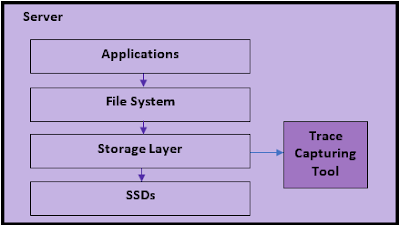
First and foremost, what is a real world workload and how do I get it? Fig. 1 shows the typical process of how a real life workload is captured.
Fig. 1. Capturing a
real-world storage workload.
Applications typically run on top of a file system that in turn push IOs to an abstracted OS storage layer before making it to the SSD. For Linux, this storage layer is the block layer, and for Windows, it can be either the DiskIO layer or the StorPort layer. IO capture tools are readily available to snoop all IOs within the storage layer. The most popular one for Linux is blktrace, and for Windows, Windows Performance Recorder is widely used capture tool. Alternatively, Workload Intelligence DataAgent (coming soon) is a powerful trace capture tool with built in intelligence to trigger and filter on user determined criteria. The outputs of these capture tools are trace files that contain all the IOs along with their timestamps and typically other information, like process IDs, CPU etc. It is these trace files that are used to generate IO replays from for offline testing.
Where can you get these IO trace files? If you work with a customer that uses your SSDs or storage subsystems, they typically collect such trace files for their own analysis purposes and may be open to sharing them. This would be the best scenario as you can get a live view of a real-world environment. If you are the SSD user, you can use the aforementioned capture tools to trace the IOs in your application environment.
Alternatively, SNIA provides a number of open-source real-life storage workloads: http://iotta.snia.org/tracetypes/3. Finally, you can always concoct your own setup- run a MySql or Cassandra database, simulate some application queries, and capture storage layer IOs. While strictly not “real-world”, this will at least give you a good sense on how application activities trickle down to storage IOs.
Replaying Workloads
With the workload traces on hand, it’s time to replay them in your test environment. The goal of doing so is to reproduce the issue that was caught during the production run, and also to tune or make fixes to SSD firmware to see if the issue gets resolved. If one is evaluating SSDs, this is a great way to see if the selected SSDs pass the workload criteria.
The recommended storage replay tool is the Workload Intelligence Replay. Replay files can be generated from Workload Intelligence Analytics, to run on an Oakgate SVF Pro appliance. The replay results can then be ported back to Workload Intelligence Analytics to compare with the original trace, or with other replay results. Fig. 2. shows the flow of how storage traces are captured, replayed, and compared.
Fig. 2. Process of
replaying and analyzing a storage trace.
When replaying a storage workload to target drive, a number of factors must be considered to make sure the replay emulates the production environment as much as possible:
- Target drive selection – Ideally, the DUT should have the same make and model as the drive that the production trace was captured on. If this is not possible and the target DUT has a different capacity, the replay software should be able to re-map LBAs so that they fit within the DUT. Oakgate SVF Pro Replay handles this situation by offering different LBA out of range policies, including skipping the IOs, wrapping the IOs, and linearly re-mapping IOs that exceed the LBA range. We’ve found re-mapping LBAs to be the most effective in duplicating production scenarios.
- Target drive prefill – It is essential the DUT gets prefilled properly to emulate the state the production drive was in before the capture happened. While it’s impossible to condition the DUT to the exact state the production drive was in, we’ve found that a simple 1x write prefill was able to duplicate production drive scenarios. Alternatively, Fiosynth offers fairly sophisticated preconditioning techniques that are reflective of data center workloads.
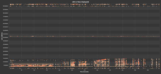
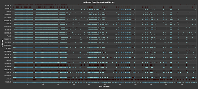
- Accurate IO timing and parameters – The heart of an effective replay is software that can emulate when and what the production host sent to the device. To achieve that goal, Oakgate SVF Pro matches the replay trace file IO in terms of relative timestamp, IO size, and LBA. Fig. 3 and 4 show the LBA vs. Time and IO Size vs. Time, respectively, of a production blktrace versus that replayed by Oakgate SVF. As can be seen, the timings and values of the replayed IOs is exactly same as the production trace. The variable of interest is typically the latency of each IO and the IO queue depth and are expected to be different from the production trace.
Replay Experiments
Now that we’ve been primed about the intricacies of workload replay, let’s take a look at some experiments.
In all experiments run, we’ve preconditioned the drive 1x. The chosen drives were standardized to 0.5 TB. All production runs were captured when the drive was formatted to 512 bytes, so for the replay, we’ve also formatted the drive to 512 bytes.
Replay Repeatability
In the first set of experiments, we tackle the question of how repeatable a workload replay is. This question is important because we need to know whether the replay software can duplicate the same profile on the same drive during a production run. Even if we can duplicate the profile, it is also crucial to know whether this same profile can be regenerated after 10s or 100s of replays. If the drive shows a statistically different profile on every replay run, it can indicate that the drive does not have very stable performance.
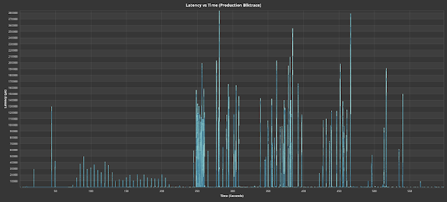
For this experiment, the production workload we are running consists of a combination of applications, primarily: Postgresql with light traffic, and Spark + HDFS data store with large datasets that get cached and persisted onto disk. We captured a blktrace on the production machine.
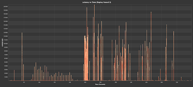
Fig. 5 shows the latency vs time of the production blktrace
over a 10 minute snapshot.
Fig. 5. Latency vs time for a production blktrace with a big
data workload
Since we control the “production” environment, we’ve taken this same drive over to an Oakgate replay appliance and ran a replay file generated from Fig. 4’s workload. We iterated multiple rounds of replay (preconditioning between each iteration) and took those results and fed it back into WI Analytics for comparison. Fig. 6 shows 3 iterations of the replay.
In a quick glance, we can see that the latency spikes and their timings for the replayed results are extremely similar to the original production trace. There are some statistical differences, if we closely, which is expected. Overall, the replays have faithfully regenerated the latency profile in an offline environment, and this particular drive has shown stable results after multiple rounds of replay.
Replay Comparison for Different SSDs
Next, let’s run experiments on how different SSDs react to the same workload. Such a use case can very well be used to qualify different drives for a data center’s set of workloads. From a different angle, the same experiment can be run on the same SSD with different firmware to see if firmware changes are effective against a particular set of workloads.
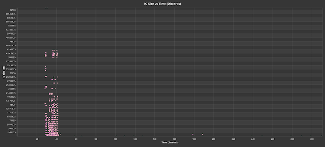
In these experiments, we had chosen an actual data center workload that showed a particularly stressful profile. Fig. 7 shows the read latency vs. time of the production workload. We can see very big latency spikes happen, and we would like to know whether other SSDs can handle this same workload without these latency spikes. Fig. 8 shows the main obstacle the workload entails – a burst of large discard (trim) IOs that is likely causing the disk to become blocked while servicing those discards, contributing the high read latency spikes.
Fig. 8. Discard (trim) IO sizes vs time for production
blktrace.
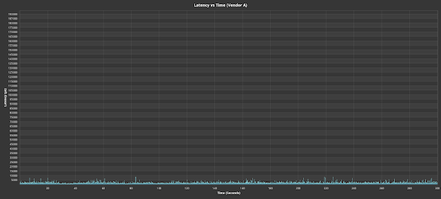
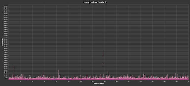
Fig. 9 shows drives from various vendors that did not
encounter the read latency spikes despite undergoing the same production
workload. Latency scales are normalized to that of the production workload the
contrast the latency differences.
By contrast, Fig. 10 shows the set of drives that show an adverse reaction to the burst of discard IOs. Vendor F in particular never recovered to its baseline latencies after getting swamped with the discard bursts.
Fig. 10. Drives that reacted adversely to the replayed
production workload.
The ability to replay production storage workloads is an essential tool to improving or qualifying SSD real-world performance. Unlike synthetic workloads, production workloads are much more unpredictable, dynamic, and reflective of real application environments. In this blog, we discuss the various aspects of accurately replaying workloads in an offline environment and showed examples on how to properly reproduce production environments. We also showed how different SSDs can react very differently to the same production workload. Hopefully, we’ve conveyed the point that it is essential to use real-world replays to design better SSDs and better match sets of SSDs relevant to one’s real-world environment.
Automotive Ethernet in the Vehicle
 |
| Figure 1 Block diagram of a typical ADAS system showing the in-vehicle networks used. |
(Click on any figure to enlarge the image.)
08 June 2021
Fundamentals of Automotive Ethernet
 |
| Figure 1: Automotive Ethernet is designed to support increasingly complex vehicle electronic systems. |
Probably the first question you ask is, “Why not just use standard Ethernet?” A summary of the fundamental features of Automotive Ethernet will show how much better Automotive Ethernet is than standard Ethernet at meeting the industry’s demand for a higher speed, robust, lightweight and lower cost data interface, one that can ultimately replace the many other protocols currently used throughout the vehicle.
01 June 2021
Five Tips to Improve Dynamic Range
Dynamic range is the ratio of the maximum signal level to the smallest signal level achievable in a measurement. Tools with good dynamic range are especially helpful for analyzing wide dynamic range signals in which a full-scale signal must be acquired, while at the same time, very small amplitude signal details must be visible. Here are five tips for improving the dynamic range of your measurement instrument.
24 May 2021
Mode Conversion
 |
| Figure 1: The lower-left and upper-right quadrants of this matrix show the S-parameters that represent mode conversion from differential to common signal, and vice versa. |
Let’s take the S-parameters SCD11 and SCD21 to see how the combination of single-ended S-parameters they represent reveal the source of mode conversion. If we look at SCD11, the reflected mode conversion, as a function of its single-ended S-parameters, we see:
17 May 2021
Converting Single to Mixed-Mode S-Parameters
 |
| Figure 1: Model of two transmission lines with crosstalk showing the transmission and crosstalk related S-parameters. |
We have introduced mixed mode S-parameters and developed a formal structure for handling them. It is now time to discuss converting single-ended S-parameters into mixed-mode S-parameters. This is important because every instrument manufacturer obtains mixed mode S-parameters by first measuring single-ended S-parameters, then converting them mathematically to mixed-mode. This assumes that the interconnects being measured are passive, linear and time invariant. Let’s begin with our model of two transmission lines with crosstalk shown in Figure 1.


