You need to test, we're here to help.

You need to test, we're here to help.

14 December 2020

Removing Reflections from DDR Signals Probed Mid-Bus

Figure 1. Virtual probing methods like VP@Rcvr can help remove reflections from signals probed mid-bus.
Figure 1. Virtual probing methods like VP@Rcvr can help
remove reflections from signals probed mid-bus.
Probing DDR signals can present some interesting challenges. The JEDEC specification indicates that all measurements should be made at the output pins of the memory chip. The challenge comes because sometimes the pins of the memory chip are not accessible. You may be able to use an interposer, but even that requires some spatial displacement from the probing point to the Ball Grid Array (BGA) pins of the memory chip. 

If the board has already been populated, there is an even greater problem because the interposer can’t be used, so probes may have to be placed in the middle of the bus in order to make a measurement. In this situation, the probe picks up signals reflected from the memory controller and the memory chip, as well as the desired signals. Reflections appear as non-monotonic ripples on the edges of DQ and DQS signals, as shown in Figure 2.

07 December 2020

Isolating DDR Read and Write Operations

Figure 1. DDR DQ and DQS signals are in phase during a Read operation and out of phase during a Write operation.
Figure 1. DDR DQ and DQS signals are
in phase during a Read operation and
out of phase during a Write operation.
Whether you are debugging or running compliance tests on Double Data Rate (DDR) or Low Power Double Data Rate (LPDDR) memory, the analysis process requires the separation of Read and Write operations to enable measurements on each distinct operational mode. 

The phase relationship between the Data (DQ) signal and the Data Strobe (DQS) signal indicates the type of operation, as shown in Figure 1.

The DQ and DQS signals are phase aligned with edges overlapping in Read mode. In Write mode, they are out of phase, and the DQS edge overlaps the center of the DQ eye.  In the lower speed versions of DDR memory devices, the measuring instrument could be triggered on this phase difference, enabling the isolation of the desired operation for testing.

30 November 2020

Oscilloscope Basics: Multiplexed Front Panel Controls

Fig. 1. Modern, slim front panel.
Fig. 1. Modern,
slim front panel.
Most Teledyne LeCroy oscilloscopes are equipped with traditional front panel controls—knobs and buttons—that are a (literally) handy way to make basic acquisition settings such as gain, timebase and trigger level. While all these could be made using the oscilloscope software, using the front panel allows you to keep dialogs closed and more of the screen “real estate” available for viewing traces as you modify these settings.

In order to optimize that real estate, front panels have become increasingly slim, and many front panel controls on newer Teledyne  LeCroy oscilloscopes are multiplexed, meaning they have multiple functions or can be used to control multiple on-screen objects. Here is a list of tips to keep in mind when using the front panel.

09 November 2020

Fundamentals of Power Integrity: Mutual Aggressors and Rail Transient Response Measurement

Fig 1. Rail droop in response to a load step is a typical case of mutual aggressors in a PDN.
Fig 1. Rail droop in response to a load step is
a typical case of mutual aggressors in a PDN.
A third type of noise found in PDNs is what we call mutual aggressors, which is crosstalk coupling from one component of the PDN onto another.

An obvious example is a load step in the PDA, where something in the system being turned on pulls current from the VRM that supplies a rail. In Figure 1, you can see how the output voltage of the VRM supplying a 1 V rail droops in response to a load step before it recovers. This is still noise: it is a signal variation that we're not expecting and don't want.

We want to be able to characterize that noise, because too much droop could affect the operation of other components that are already consuming power from that device.

In order to do so, we’re going to measure the rail transient response to the load application. We need only look at two signals: the voltage and the current on the rail of interest. Figure 1 shows the voltage on C5 (the green trace) and the current on C8 (the orange trace).

02 November 2020

Your Ground Bounce Questions Answered

Figure 1. Line set to "quiet low" shows ground bounce occurring as I/O driver switches.
Figure 1. Line set to "quiet low" shows ground
bounce occurring as I/O driver switches.
During an October 2020 webinar, Don’t Let Ground Bounce RuinYour Day, Dr. Eric Bogatin was asked several questions regarding his topic of presentation. Here are his answers.

Q: From what frequency should we consider ground bounce to be a problem?

A: Ground bounce is really due to a dI/dt. Generally, it becomes a problem with rise times shorter than 100 ns. The bandwidth of this is about 3.5 MHz. This means ground bounce can be an issue at relatively low frequency.

19 October 2020

Which Virtual Probing Method to Use?


Virtual probing lets you "probe" where a probe can't reach, or compensate signals by deembedding or simulating devices and channels.
Virtual probing lets you "probe" where a probe
can't reach, or compensate signals by deembedding
or simulating devices and channels.
A great feature of Teledyne LeCroy oscilloscopes is the ability to apply virtual probing to compensate an input signal, whether by deembedding fixtures from the signal path, or simulating a “missing” component. It is especially helpful in cases where the signal is difficult to probe at the ideal location, hence the concept of “virtual” probing.

For example, because the JEDEC electrical specifications are defined at the balls of the DDR DRAM, it is often necessary to use the virtual probing capabilities of the oscilloscope to get the best representations of DDR signals to be analyzed with DDR Debug Toolkit or QualiPHY compliance software.

Here, we’ll give an overview of the virtual probing methods that become available with the installation of the SDAIII-CompleteLinQ or VirtualProbe software options, and some guidance as to which method is best to use in which case. And although we’ll show examples drawn from DDR analysis, the benefits of virtual probing are by no means limited to DDR signals.

21 September 2020

Fundamentals of Power Integrity: Board Pollution

Figure 1. "Pollution" occurring on PDN traces.
Board pollution is noise occurring on the packages and interconnects (traces and planes) that carry current from the VRMs to the consumer devices.
One place it can originate is from the VRM itself, for example, with the switching noise the VRM generates (Figure 1). That can be a real concern if the board capacitance means you have a resonance around the switching frequency that would act as an amplifier for the switching noise and cause all kinds of problems with other devices on the board.

14 September 2020

Fundamentals of Power Integrity: Self-aggression Noise

Fig. 1: VRM-switching noise is a self aggressor that can be identified because it is synchronous with the PWM clock.
Fig. 1: VRM-switching noise is a self aggressor that can be
identified because it is synchronous 
with the PWM clock. 
Self-aggression noise is so-called because it is inflicted by a component onto itself through its normal operation; nothing else in the system is affecting it. When we look for this, we want to ensure the system is in a steady state, in a place where the noise environment is fairly clear (e.g., the device is on an evaluation board).

An example of self-aggression would be VRM-switching noise. Figure 1 shows ripple on a 900 millivolt rail (yellow trace) at a time when no load is present. One of the things that tells us this is switching noise is that it is synchronous to the PWM clock (red trace). Ripple that is synchronous with the switching clock is a typical figure of merit for identifying switching noise.

31 August 2020

Fundamentals of Power Integrity: Characterizing PDN Noise

Figure 1. Noise tolerances for embedded system components are becoming ever tighter.
Figure 1. Noise tolerances for embedded system
components are becoming ever tighter.
Power integrity concerns maintaining the quality of power from generation to consumption in an embedded system. “Good” power integrity could be defined as having noise levels that are within tolerance. This short series will focus on characterizing noise on your power delivery network (PDN), with the goal of knowing where you must adjust your design to meet those tolerances.

Why do we care about voltage rail noise? As electronic designs strive for ever lower power consumption, power rails already carry very low voltages, often 1 V or less. Components like RF receivers, ADCs and DACs can be affected by noise of less than 1% of the rail value (Figure 1). This means noise tolerances can be as tight as single-digit millivolts, which is why power integrity takes up considerable validation time in labs.

24 August 2020

How to Connect the Returns to an Unshielded Twisted Pair

Figure 1. Three options for connecting a TDR to a UTP.
During a recent webinar, Dr. Eric Bogatin was asked several questions about how to measure unshielded twisted pairs (UTPs), which are differential pairs with no return path. Here is his answer to one of the questions. For more information, check out the whole webinar on Differential Pairs with No Return Paths.

Q: For the UTP measurement, do you need to connect the SMA connector shield grounds together?

A: Yes. It’s very important to make sure the grounds are connected at the cable connectors.

There are really three ways the connections can be made from a differential TDR to the UTP cable. These three options are shown clockwise from left to right in Figure 1.

03 August 2020

How to Choose Between the Oscilloscope's 50 Ohm Input and 1 MOhm Input

Dr. Eric Bogatin

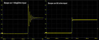
Fast buffered signal over a 1 megaohm input, and same signal over 50 ohm input
Figure 1. The same signal from a fast-buffer driver
measured with a 1-meter, 50 ohm cable with
1 megaohm input to the scope, and
same cable with 50 ohm input to the scope.
When every oscilloscope has both a 50 Ohm input and a 1 MOhm input, how do you choose which one to use? Here are my recommendations for when each input should be used. 

For additional information on this topic, check out my webinar on What Every Oscilloscope User Needs to Know About Transmission Lines.  

27 July 2020

Fundamentals of 100Base-T1 Ethernet

100Base-T1 toplogy
100Base-T1 Topology
The term Automotive Ethernet can be used to refer to any Ethernet-based network for in-vehicle electrical systems. It encompasses 100Base-T1, as well as several other variants/speeds of Ethernet (e.g., 10Base-T1, 1000Base-T1). Here, we’ll describe 100 Mb/s Automotive Ethernet as defined by the IEEE in its 802.3bp specification, which is nearly identical to Broadcom’s variant, BroadR-Reach.

20 July 2020

What Is SENT SPC?


Decoding of SENT SPC frames showing Master Trigge Pulse.
SENT SPC interrogation mechanism showing 
MTP preceding standard SENT frame.
Single Edge Nibble Transmission protocol, more commonly known as SENT (SAE J2716 JAN201604), has long been used by the Automotive industry to report low-speed sensor data to the Engine Control Unit (ECU). SENT was developed because the environment in a car was too noisy to transmit high resolution (10- or 12-bit) sensor data vertically on a 5 V bus. Instead, sensor signals are transmitted as a series of pulses, with data measured by falling-edge to falling-edge times. Information lies within the width of the pulses. Later specifications of SENT introduced Fast and Slow Channels to designate different streams of information carried within the same messages.

06 July 2020

Probe Safety Demystified: Dynamic Range and Voltage Swing

One of the most basic things to know when using any probe is “what is the maximum voltage the device can safely measure?” The answer isn’t as straightforward as you might imagine, it requires understanding several key probe specifications as well as the nature of your signal.

Single-ended Range

Single-ended range is maximum voltage input to ground.
Figure 1. Single-ended range is
measured voltage input to ground.
Everyone is pretty familiar with single-ended range: that's the maximum safe voltage input to ground, shown in Figure 1. Ground is directly tied to oscilloscope ground, which is tied to building ground. Therefore, when measuring voltage within this range using a single-ended probe, the ground connection cannot be a floating voltage, or you could damage the probe, the DUT, the oscilloscope...maybe yourself, as well. Single-ended voltage must be a grounded voltage on your board or something that could be tied to ground.

29 June 2020

Probe Safety Demystified: CAT Ratings

Measurement Category (CAT) ratings by type of circuit probed.
Figure 1. CAT ratings required to
safely test different electrical sources.
(Sourced from “Measurement Categories,”
Wikipedia, Oct. 28, 2019.)
Any voltage probe will have several published specifications that are meant to indicate under what circumstances that probe is safe to use. They answer questions such as “What is the maximum voltage I can safely run through this probe?” and “Can I safely hold this probe while using it, or does it need to be mounted somewhere far away?” In this post, we’ll explain what the CAT rating is telling you.

CAT ratings are standardized ratings used to categorize the suitability of a voltage measurement device based on the source impedance of what it is used to measure. They are issued by the International Electrotechnical Commission (IEC).

22 June 2020

Build Your Own Low-Cost Power Rail Probe

Source series termination of a coaxial cable is a low-cost alternative for probing low-voltage, high-bandwidth signals.
Figure 1: The source series termination method is
a low-cost alternative for probing low-impedance,
fast-switching sources.

In an earlier post, we discussed the limitations of  Using 50-Ohm Coax from DUT to Oscilloscope  with low-voltage, high-bandwidth signals, like power rails. In this post, we’ll explain how to build your own, low-cost power rail probe to serve the purpose.

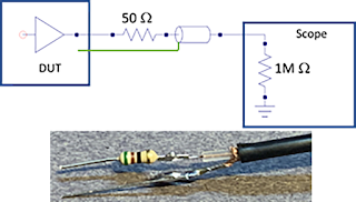
The source series termination method is a good alternative for probing a low-impedance, fast-switching source, comprising a 50-ohm resistor in series between the DUT and the coaxial-cable connection. The coaxial cable is then connected to the oscilloscope’s analog input set for 1 megaohm termination. An equivalent circuit model and a simple implementation appears in Figure 1.

15 June 2020

What Every Oscilloscope User Needs to Know About Transmission Lines

Eric Bogatin, Signal Integrity Evangelist, Teledyne LeCroy

Measured voltage at the oscilloscope from a fast edge, low impedance DUT, with the oscilloscope at 1 megaohms (left) and 50 ohms (right).
Figure 1. Measured voltage at the oscilloscope from a
fast edge, low impedance DUT, with the oscilloscope at
1 megaohms (left) and 50 ohms (right).
It is easy to take a measurement with an oscilloscope and see a voltage waveform on the screen. It is sometimes hard to take a measurement without artifacts and interpret all the details of the measurement. 

Whenever you measure a signal with a rise time shorter than about 20 ns, assuming a 1 m long coax cable, transmission line effects should pop to the top of your list of potential artifacts to consider and avoid. 

08 June 2020

Charting High-Resolution Oscilloscope Performance


Eric Bogatin, Signal Integrity Evangelist, Teledyne LeCroy

Signal measured by 8-bit and 12-bit oscilloscope.
Figure 1. 8-bit vs. 12-bit oscilloscope waveforms.
There are hundreds of different oscilloscope models from a dozen different vendors. How do you make sense of all of their different features to pick the one instrument right for your application?  Here is a simple way of comparing high-resolution oscilloscopes.

High-resolution usually refers to the vertical resolution, the quantization of a waveform into a fixed number of vertical levels measured by the oscilloscope's Analog-to-Digital Converter (ADC). The more bits of vertical resolution, the more levels and the more detailed the waveform rendered. The earliest digital storage oscilloscopes (DSO) started as 8-bit resolution, or 256 vertical levels. But in the last ten years, as ADC chip technology got faster, higher resolution appeared in the industry, pioneered by Teledyne LeCroy.  Now, many oscilloscopes come with 10-bit and 12-bit vertical resolution. Why would you want higher resolution? The answer: the ability to see lower level signals and better dynamic range. An example of the difference between the same signal measured with an 8-bit and 12-bit oscilloscope is shown in Figure 1. 

01 June 2020

USB4 Electrical Testing: Where Are We?

Preliminary drafts of the USB4 Compliance Test Specifications (CTS) were released to USB-IF work group members in early 2020 covering the electrical through protocol layer testing of USB4 router assemblies captive cable devices. These CTS documents define the required testing for USB4 hosts, hubs, and peripherals that make up the USB4 ecosystem.  Thunderbolt 3 (TBT3) is also supported in USB4 end products and is tested using the existing TBT3 Host/Device CTS.

While the electrical test methodologies are similar to previous USB 3.2 compliance tests, USB4 is largely based off the TBT3 physical layer, and these test methods have been adopted. Here, we summarize the USB4/TBT3 test approach called out in the aforementioned documents.

USB4 Transmitter Testing

Figure 1. Test points TP2 and TP3 for USB4 Electrical Compliance Testing (Source: USB-IF)
Figure 1. Test points TP2 and TP3 for USB4
Electrical Compliance Testing (Source: USB-IF)
Presently, there is no SIG-TEST software for performing transmitter (Tx) testing, although it is anticipated that one will be released by the USB-IF in the future. All Tx tests performed by QPHY-USB4-TX-RX utilize Teledyne LeCroy methods, with measurements made directly by the oscilloscope.

Figure 1 shows the Test points defined in the CTS for physical layer testing. Testing of the Tx-side is  similar to those performed for USB 3.2 in that the signal is captured at the connector (TP2), where many measurements are defined. Then, a passive cable model is embedded and equalization is applied to result in TP3 measurements.

27 May 2020

Reading S-parameters: Sharp Dips

Figure 1. A resonant cavity composed of two interior layers on a four-layer printed circuit board.  The return current from the signal path couples into the plane cavity and excites its resonance modes.
Figure 1. A resonant cavity composed of two interior layers
on a four-layer printed circuit board.  The return current from
the signal path couples into the plane cavity and excites its
resonance modes.
The last pattern we'll cover in this series on reading S-parameters is sharp dips. These dips result from coupling to high-Q resonant structures and represent very narrowband absorption in S21 or S11.

Where do you see resonant coupling? Resonant structures can include coupling to an interconnect that is floating and not terminated. The structure does not have to be a uniform transmission line, it can also be a cavity made up of two or more adjacent plates as shown in Figure 1. Commonly, when a signal goes through a cavity and we hit the resonances of the cavity, it absorbs energy and results in narrow dips in the S-parameters.

18 May 2020

Reading S-parameters: Broad Dips

Figure 1. Quarter wave stubs exhibit resonance which impacts S21 as broad dips.  The resonant frequency can be computed based on the characteristics of the transmission lines and its length.
Figure 1. Quarter wave stubs exhibit resonance which
impacts S21 as broad dips.  The resonant frequency
can be computed based on the characteristics
of the transmission lines and its length.
Besides ripples and monotonic drop offs, the third pattern commonly seen in plots of S-parameters are broad dips due to stub resonances. Figure 1 shows an interconnect which includes a stub.  The interconnect is composed of 50 ohm uniform transmission lines which incorporate a branch point with an open at the end. 

Not surprisingly, the open stub is a discontinuity. What's going to happen? At the open, it's going to reflect and head back. At the junction, it's going to branch. Some of it's going to go back toward the source and some of it's going to go forward toward the receiver.

11 May 2020

Reading S-parameters: Monotonic Drop Offs

Figure 1. As a signal propagates, the amplitude drops off exponentially with distance due to signal losses.
Figure 1. As a signal propagates, the amplitude drops off
exponentially with distance due to signal losses.
Last week, we showed how ripple in S-parameters relates to the length of the interconnect. The second common pattern we see when reading plots of S-parameters is the monotonic drop off in the amplitude of the transmission coefficient (S21), commonly referred to as the insertion loss. If we apply a sine wave and look at its amplitude as it moves through that interconnect, we see that it drops off exponentially as shown in Figure 1.

V_Out is shown as V_In times a decaying exponential. (Note that attenuation is usually described using base 10 rather than base e).

04 May 2020

Reading S-parameters: Ripples

Ripples in s-parameters show impedance discontinuities
Figure 1. Ripple patterns commonly seen in S11 and S21.
When we look at plots of S-parameters, we can observe four classic patterns that affect the S11 reflection coefficient (aka. return loss) and the S21 transmission coefficient (aka. insertion loss): ripples, monotonic drop offs, broad dips and sharp dips. In this post, we’ll look into how the characteristics of the interconnect affect the ripple pattern, which will help you better understand your own measurements. 
The ripples in S11 and sometimes in S21 in Figure 1 are due to reflections in the interconnect caused by impedance discontinuities. This phenomenon has been investigated in an earlier post, What S-parameters Reveal About Interconnects (Part III)

27 April 2020

PCIe Electrical Testing: Where Are We?

PCIe specifications through Rev 5.0
Figure 1. PCIe specifications through Rev 5.0.


You may be wondering where we are in the roll out of PCI Express test specifications and active testing. Figure 1 shows the status as of March, 2020.

16 April 2020

Six Ways Not to be Confused by S-parameters (Part II)

In Part I, we discussed three causes of confusion when working with S-parameters and what you can do to avoid them.  In this post, we’ll discuss three more ways not to be confused by S-parameters.

4. Know the difference between return loss and reflection coefficient

Figure 1. A 2-port device has two distinctly interesting S-parameters, S11 and S21.  S11 is the reflection coefficient of Port 1 (also called return loss), and S21 is the transmission coefficient of Port 2 (also called insertion loss).
Figure 1. A 2-port device has two distinctly interesting
S-parameters, S11 and S21.  S11 is the reflection
coefficient of Port 1 (also called return loss), and
S21 is the transmission coefficient of Port 2
(also called insertion loss).
Let’s start by looking at a 2-port device illustrated in Figure 1.

There are two S-parameters of interest in a 2-port device.  The first is the reflection coefficient, S11, that measures the ratio of the reflection from Port 1 to the drive signal at that port.  The second is the transmission coefficient, S21, that is the ratio of the output of Port 2 to the drive signal into Port 1.  Confusion arises because historical measurements of return loss and insertion loss are often used interchangeably with reflection coefficient and transmission coefficient, respectively.

13 April 2020

Six Ways Not to be Confused by S-parameters (Part I)


S-parameters describe the electrical properties of electronic interconnects, which can include connectors, printed circuit traces and vias, cables, and oscilloscope probes. Given that instruments such as Teledyne LeCroy’s WavePulser 40iX make measuring S-parameters relatively simple, there are still some aspects of S-parameters that can cause confusion, especially to new users. Here are six things you can do to avoid confusion when working with S-parameters.

1. Know where the fixture ends and the DUT begins

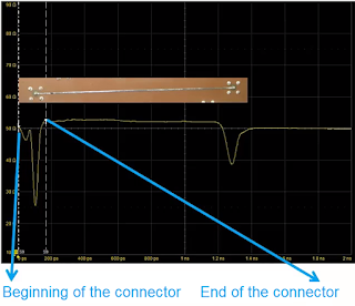
Connectors needed to make a measurement add their own characteristics to the measurement.
Figure 1. Characterizing a  microstrip line requires
two connectors, one at each end of the line. 
These connectors add their own characteristics to
the measurement. A TDR measurement can
determine the boundary between the connectors
and the microstrip PC line. 
Measuring S-parameters involves connecting a test instrument to the Device Under Test (DUT), placing the DUT in series with a number of other interconnect elements, as in Figure 1. The DUT is not isolated, and confusion can arise as to where you want the cables and fixtures to end and where the DUT begins. Do you want the DUT to include just the cable of the DUT? What about the connectors on its ends? What about the matching fixture or lead in in the circuit board?