 |
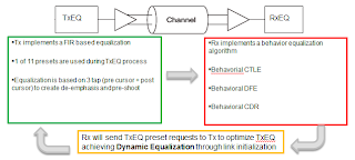
| Figure 1: An overview of the elements of PCIe 3.0 dynamic link equalization |
On the transmit side of the channel is a three-tap finite impulse response (FIR) filter with three settable cursor coefficients; these cursors determine the level of de-emphasis and preshoot before the signal enters the channel. As discussed in our last post, presets may be applied to these settings. On the receive side, a behavioral equalization algorithm comprises continuous time linear equalization (CTLE), decision feedback equalization (DFE), and clock/data recovery (CDR). This algorithm may equalize the signal after it has traversed the channel (Figure 1).
 |
| Figure 2: Main state diagram for an LTSSM |
In the PCI-SIG's language, two PCIe devices exchange "training sequences" to negotiate a number of link parameters, including elements such as lane polarity, link/lane numbers, equalization, data rate, and so on. The way this happens is through the execution of a link training and status state machine (LTSSM), which is depicted in Figure 2. When a PCIe add-in card is plugged into a system and everything is powered up, the LTSSM will be implemented in the order of the blue-circled states. The Recovery state includes a number of substates shown in Figure 3, one of which is recovery.equalization (outlined in green). That is where all the link training takes place to adjust the equalization parameters for that particular channel.
 |
| Figure 3: The Recovery substates |
Inside of recovery.equalization are four stages of the link tuning and equalization, labeled Phases 0 through 3 (Figure 4), enabling both sides of the link to advertise their capabilities and get into the training process. A starting-point preset is the entry to further tuning of the link, so the system provides that to the add-in card while still at 2.5 GT/s.
Phase 0 starts at a rate of 2.5 GT/s. The system (upstream) sends a speed-change request along with a TxEQ preset to the add-in card (downstream). That preset is to be used when the add-in card first jumps to 8 GT/s. In this fashion, the system can establish communication with a bit-error rate of at least 10-4
 |
| Figure 4: A diagram of the four phases of recovery.equalization |
When all of the above is accomplished and we exit out of recovery.equalization, we should be at the optimal TxEQ and RxEQ on both sides of the link and should be operating at a BER of at least 10-12.
In the next installment of this series of posts on PCIe 3.0 dynamic link equalization, we'll take a closer look at the meat of the process, which occurs in Phases 2 and 3 of recovery.equalization.
2 comments:
Where is the next installment on the series. I can't find it?
The next post is here: http://blog.teledynelecroy.com/2018/01/an-under-hood-view-of-pcie-30-link.html
Post a Comment