31 January 2018

Getting The Most Out Of Your Oscilloscope: Tracks and Trends

The track math function shows how data changes over time
Figure 1: The track math function
shows how data changes over time
Our discussion of cursors and parameters leads us neatly into the topics of tracks and trends, which are both means of extending parameter measurement into a more analytical direction. We can do this using math functions that are part of your Teledyne LeCroy oscilloscope's toolset.

30 January 2018

Getting The Most Out Of Your Oscilloscope: Cursors and Parameters
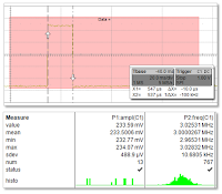
Cursors (top) and parameter measurements (bottom) are both powerful tools in their own right
Figure 1: Cursors (top) and parameter
measurements (bottom) are both
powerful tools in their own right
Oscilloscopes give us a wealth of tools with which to view, measure, and analyze the performance of a circuit. Broadly speaking, two classes of such tools are cursors and parameter measurements. Taken on their own, both classes afford the user a great deal of capability. Put them together, though, and you can really start to gain deep insights into what's going on with a waveform.

29 January 2018

Getting The Most Out Of Your Oscilloscope: Documentation

A LabNotebook entry quickly and easily saves everything you need to later replicate your measurements
Figure l: A LabNotebook entry quickly and easily saves
everything you need to later replicate your measurements
If we really want to get the most out of our oscilloscopes, we'd be remiss in overlooking the documentation capabilities that modern instruments provide. It's so important to document our working sessions so they're consistent and repeatable. Oscilloscope setups can be quite intricate for a given measurement or procedure. Why not let the instrument help us keep track of such things?

Getting The Most Out Of Your Oscilloscope: Trigger Delay

Pre-triggering, or trigger delay, is a useful tool for debugging applications
Figure 1: Pre-triggering, or trigger delay, is a useful tool for
debugging applications
Triggering is one of the most basic, yet most useful, tools your oscilloscope offers you. Say you want to see what led up to, and/or what follows, a trigger condition. You're looking at an interesting waveform such as that shown in Figure 1. You have the trigger's delay position set at 10% and 90%.

26 January 2018

Getting The Most Out Of Your Oscilloscope: Navigation With MAUI

Oscilloscope UIs such as Teledyne LeCroy's MAUI provide tons of shortcuts and touch gestures
Figure 1: Oscilloscope UIs such as
Teledyne LeCroy's MAUI provide
tons of shortcuts and touch gestures
Today's real-time digital oscilloscopes are easier to use than their predecessors, and new models get easier all the time. Oscilloscopes often are equipped with touch screens and elaborate user interfaces that provide a plethora of shortcuts and smartphone-like touch gestures that make common operations extremely fast and easy.

Getting The Most Out Of Your Oscilloscope: Setup

Choosing a effective sample rate is key to seeing the finer details of a waveform
Figure 1: Choosing a effective sample rate is key
to seeing the finer details of a waveform
Today's real-time digital oscilloscopes are so packed with bells and whistles (or "features," if you prefer) that you can forget how to use many of them. In fact, you might not even realize some exist! But they're all there for a reason, and they're all useful, maybe even more so than you know. To that end, we'll take a tour of a typical Teledyne LeCroy oscilloscope's features and give you some pointers as to how, and when, you can best take advantage of them.

24 January 2018

Making On-Die Power-Rail Measurements (Part III)

This screen capture shows the idle-state conditions
Figure 1: This screen capture shows
the idle-state conditions
Having reviewed the test setup for on-die power-rail testing and our expectations of what the tests should show us, let's walk through the measurements and look over the results. We'll also note whether our results align with our expectations or are outside of those expectations.

Making On-Die Power-Rail Measurements (Part II)
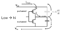
When switching from low to high, PDN noise flows from the Vdd rail through to the Vss rail
Figure 1: When switching from low to
high, PDN noise flows from the Vdd
rail through to the Vss rail
Now that we're ready to begin some on-die power-rail measurements, it's a good idea to step back for a moment and anticipate what these measurements should show us. What actually happens on the die when CMOS gates are switching on and off? What should we expect to see on the on-die power rails? And what happens at the clock edges?

Making On-Die Power-Rail Measurements (Part I)

Our test setup for the on-die measurement examples
Figure 1: Our test setup for the
on-die measurement examples
Our exploration of on-die power-rail measurements has brought us to the point of demonstrating some examples of these measurements. As noted in the prior post, we will use an Atmel 328 microcontroller demo board, prepared with firmware to control it explicitly for our purposes, and with coaxial cable in place on the bottom of the board to serve as transmission lines for our signals of interest.

Measuring Shared On-Die Power Rails


This schematic represents the signal paths  in typical, general-purpose I/Os
Figure 1: This schematic represents the signal paths
in typical, general-purpose I/Os
If you're taking power-rail measurements on a semiconductor die that is appropriately instrumented with sense lines and a direct connection to the die's core PDN, you're in pretty good shape. But what if that's not the case? If the die's I/O power rails are shared by the core power rails, here's a way to get your core power-rail measurements anyway.

22 January 2018

Setting the Stage for On-Die Power-Rail Measurements

Measuring on-die Vdd rail noise requires a suitably instrumented die and package
Figure 1: Measuring on-die Vdd rail noise requires
a suitably instrumented die and package
Armed with a suitable oscilloscope and active voltage-rail probe, you're now ready to make some power-rail measurements on a semiconductor die. Of course, making measurements on a die is a little different than making measurements on a printed-circuit board. This is where careful design-for-test at the die level comes in, because the chip, its packaging, and the board on which it will be mounted must be instrumented so as to make the on-die measurements possible.

Power-Rail Noise: Small Signal, Big DC Offset

Your scope's vertical adjust has its limits
Figure 1: Your
scope's vertical
adjust has its
limits
We've been working through the various challenges in making power-rail noise measurements. One of those challenges is RF pickup that can often swamp the noise signal, and the way around that is to ensure a coaxial connection from the oscilloscope's input down to the power rail itself. We want a high signal-to-noise ratio (SNR), so we're better off with a 1X probe than with a 10X attenuating probe. We want high bandwidth, so we want a 50-Ω termination at the oscilloscope input.

19 January 2018

Bandwidth vs. Current Load in Power-Rail Measurements

Connecting a 6" length of coaxial cable between a low-impedance DUT and a 1-MΩ produces ringing artifacts on your signal acquisition
Figure 1: Connecting a 6" length of coaxial cable between
a low-impedance power rail and a 1-MΩ input impedance
produces reflections and ringing artifacts
on your signal acquisition
Among the various challenges we've discussed in measuring noise on power rails are RF pickup and signal-to-noise ratio (SNR). Here's another: how do you achieve high bandwidth in your measurements while also minimizing current load on your DUT? Given that your DUT is a power rail, you really don't want to draw too much current from it. But these two measurement criteria are at loggerheads with each other. It's a quandary, and it has to do with the fundamental nature of signals on interconnects.

18 January 2018

How 10X Attenuating Probes Kill Signal-to-Noise Ratio

Figure 1: Signal waveforms captured using a 10X attenuating
probe (top) and a BNC probe (bottom) with tips open
We've begun discussing things that can derail (see what we did there?) your power-rail measurements, such as the deleterious effects of RF interference. In the same context, one should always be mindful of certain characteristics of oscilloscope probes; namely, the 10X attenuating probes that are often lying around on the testbench.

Understand RF Pickup When Measuring Power Rails

Teledyne LeCroy's  HDO8108A sports a very low  noise floor of about 145 μV
Figure 1: Teledyne LeCroy's
HDO8108A sports a very low
noise floor of about 145 μV 
Measuring the noise on a power rail seems to be a straightforward task. However, there are some basic pitfalls that can cause incorrect, or even downright strange, results. Let's look at one of these challenges: RF pickup. We'll demonstrate the effect of RF pickup on a power-rail measurement, and then we'll show you an effective means of mitigating that effect.

17 January 2018

Some More PCIe 3.0 Test Examples (Part II)
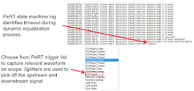
This shows how a PeRT 3 state-machine log can be invaluable in diagnosing timeouts in requests for presets
Figure 1: This shows how a PeRT 3 state-machine log can be invaluable
in diagnosing timeouts in requests for presets
Continuing on from our last post, let's look at some more examples of common PCIe 3.0 test scenarios and how a well-equipped PCIe 3.0 testbench would approach them. Recall, if you will, that such a testbench would comprise a real-time digital oscilloscope of suitable bandwidth (such as Teledyne LeCroy's SDA830Zi-B oscilloscope), a protocol-enabled receiver tester (such as Teledyne LeCroy's PeRT 3 Phoenix System), and software that enables simultaneous, correlated views of the protocol and physical layers (such as Teledyne LeCroy's ProtoSync software).

Some PCIe 3.0 Test Examples (Part I)

Protocol and electrical views of  slow electrical response to a preset request
Figure 1: Protocol and electrical views of
slow electrical response to a preset request
We took a tour of a typical PCIe 3.0 testbench setup in a recent post. Now, let's see that testbench in action with some application examples of some common bad behavior one might encounter from a PCIe 3.0 channel. These include: slow electrical response, slow protocol response, and so on.

A Tour of a PCIe 3.0 Test Setup

Test-equipment requirements for PCIe 3.0
Figure 1: Test-equipment requirements for PCIe 3.0
Having examined the complex machinations of PCIe 3.0 dynamic link equalization in earlier posts (see the links below), now we will look at a typical test setup for design and debug and/or compliance testing. Then we will move on to some test examples showing some common problems that one might encounter.

16 January 2018

An Under-The-Hood View of PCIe 3.0 Link Training (Part II)

A diagrammatic view of the PCIe 3.0 dynamic link training process
Figure 1: A diagrammatic view of the
PCIe 3.0 dynamic link training process
Our last post in this series began examining the recovery.equalization process of PCIe 3.0 dynamic link training, beginning with Phases 0 and 1 of the process (Figure 1). Next, we will move on to take a closer look at Phases 2 and 3, where we'll see what can happen with devices in which the algorithms are not up to par. Namely, issues such as packet errors, dropped packets, and link retraining at lower data rates than 8 Gb/s.

PCIe 4.0 PLL Bandwidth Testing

PLL bandwidth testing ensures that the add-in card's PLL bandwidth and peaking are within specifications
Figure 1: PLL bandwidth testing
ensures that the add-in card's
PLL bandwidth and peaking
are within specifications
The final piece of the PCIe 4.0 compliance-test puzzle—at least until PCI-SIG completes its test definitions—is the PLL bandwidth test. This test, which is performed only on add-in cards, verifies that the PLL bandwidth and peaking are within the limits allowed by the PCIe 4.0 specification (Figure 1).

15 January 2018

PCIe 4.0 Receiver Link-Equalization Testing (Part II)

Working out the optimal combination of Tx emphasis presets and receiver CTLE settings
Figure 1: Working out the optimal combination of Tx emphasis
presets and receiver CTLE settings
As may be apparent from our previous post on PCIe 4.0 receiver link-equalization testing, this part of the PCIe 4.0 compliance tests is somewhat involved. When we left off last time, we were in the midst of receiver calibration, looking to ensure that the test-signal eye is as closed as possible without violating the specification limits.

PCIe 4.0 Receiver Link-Equalization Testing (Part I)

PCIe 4.0 receiver link-equalization testing takes place at the site of the channel's worst-case signal
Figure 1: PCIe 4.0 receiver link-equalization testing
takes place at the site of the channel's worst-case signal
In the battery of PCIe 4.0 compliance tests, there is but a single test of receiver behavior: Rx link-equalization testing. Given that our DUT in this test is an add-in card, we want to have our worst-case signal at the Card ElectroMechanical (CEM) connector (Figure 1). The signal then proceeds through the channel on the add-in card to the end point, which is the receiver on the DUT.

PCIe 4.0 Transmitter Link-Equalization Testing

Shown is an overview of the PCIe 4.0 link-equalization response test
Figure 1: Shown is an overview of the PCIe 4.0
link-equalization response test
PCI Express has seen steady, and significant, increases in bit rates in each generational revision. Most recently, bit rates leaped from 8 Gb/s in PCIe 3.0 to 16 Gb/s in the current version 4.0. With these speed increases has come the need for dynamic link equalization, which becomes necessary for the sake of signal integrity. Compliance tests for dynamic link equalization is where things start to get a little more sophisticated, particularly when it comes to PCIe 4.0

12 January 2018

PCIe 4.0 Transmitter Electrical Testing (Part II)

With an add-in card as our DUT, we will measure the transmit signal at the root complex on the system board
Figure 1: With an add-in card as our DUT, we will measure
the transmit signal at the root complex on the system board
With PCIe 4.0 compliance workshops close at hand, let's get familiar with the compliance test process. We've set the stage for electrical transmitter tests by describing the PCIe 4.0 nominal channel and also reviewed the test-equipment requirements; now we'll begin examining the tests in some detail. The two basic transmitter tests are the preset test and signal-quality test.

PCIe 4.0 Transmitter Electrical Testing (Part I)

The two basic PCIe 4.0 transmitter tests outlined in green
Figure 1: The two basic PCIe 4.0 transmitter tests
are shown above outlined in green
You've been introduced to some of the background and history that has brought the PCI Express protocol standard to its fourth generation, and we've discussed the test-equipment requirements for PCIe 4.0 electrical compliance testing. Let's begin examining the compliance testing, beginning with transmitter electrical tests.

11 January 2018

Gearing Up for PCIe 4.0 Electrical Compliance Test

Figure 1: A key element in PCIe 4.0
compliance test is a high-bandwidth,
real-time oscilloscope (shown is the
Teledyne LeCroy LabMaster 10Zi-A)
Armed with some of the background information and history on PCIe 4.0 electrical compliance testing, we're now ready to look at just what it takes in terms of test equipment to determine compliance for a PCIe 4.0 device. With the increase in data-transfer rate from 8 Gb/s in PCIe 3.0 to 16 Gb/s in PCIe 4.0, so too have the test equipment requirements advanced.

Introduction to PCIe 4.0 Electrical Compliance Test

PCIe logo
Figure 1: PCI Express is now in its fourth generation
and poses daunting physical-layer test challenges
The Peripheral Component Interface Express standard (PCI Express, or PCIe) has been with us for some 14 years now, a pretty good run by computer-industry standards, and it shows no signs of fading away anytime soon. Now in its fourth generation, which sports data-transfer rates up to 16 Gb/s, PCIe presents daunting physical-layer test requirements (Figure 1).

04 January 2018

Probing Techniques and Tradeoffs (Part VI): Dynamic Range

Differential-mode dynamic range is the maximum allowable voltage between the probe amplifier's inputs
Figure 1: Differential-mode dynamic range is the maximum
allowable voltage between the probe amplifier's inputs
We've been discussing probe loading, which is the unavoidable reality of what happens when you attach an oscilloscope probe to a live circuit. We'll now shift the discussion to dynamic range, an important topic that can be overlooked when selecting an oscilloscope probe. There are three types of dynamic range that one should understand. Each of them will influence how you set up your probe and how you set up your signal under test to most effectively get that signal into the oscilloscope's front-end amplifier.