 |
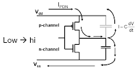
| Figure 1: When switching from low to high, PDN noise flows from the Vdd rail through to the Vss rail |
When the P-channel device (or any gate on the die, for that matter) switches from logic low to logic high, noise from the power-distribution network (PDN) on the die will flow from the Vdd/Vcc rail all the way through to the Vss rail (Figure 1). This is because the capacitance of the output line is referenced to the capacitances of both rails when the device switches from low to high.
 |
| Figure 2: When switching from high to low, PDN noise still flows through the impedance of the PDN |
 |
| Figure 3: Expect to see asymmetry in the current draw as clock edges rise and fall. |
In looking at both edges of the clock, we expect to find that when the clock turns on, all the gates are typically edge-switched. Generally speaking, depending on the logic design, when the clock edge rises, the gates are switched, and when the clock edge falls, the gates are latched. In latching, there should be less current draw than in switching. So even though we get PDN current flowing between Vdd/Vcc and Vss on both clock edges, there should be an asymmetry in that current flow (Figure 3).
That sums up our expectations of what we should see on the on-die power rails. Next time, we'll look at the actual measurement results.
Previous posts in this series:
Understand RF Pickup When Measuring Power Rails
How 10X Attenuating Probes Kill Signal-To-Noise Ratio
Bandwidth vs. Current Load in Power-Rail Measurements
Power-Rail Noise: Small Signal, Big DC Offset
Setting the Stage for On-Die Power-Rail Measurements
Measuring Shared On-Die Power Rails
Making On-Die Power-Rail Measurements (Part I)
No comments:
Post a Comment